
Competitive Price China cardboard Milling board
PCB Milling
Printed circuit board milling (also: isolation milling) is the process of removing areas of copper from a sheet of printed circuit board material to recreate the pads, signal traces and structures according to patterns from a digital circuit board plan known as a layout file. Similar to the more common and well-known chemical PCB etch process, the PCB milling process is subtractive: the material is removed to create the electrical isolation and ground planes required. However, unlike the chemical etch process, PCB milling is typically a non-chemical process and as such it can be completed in a typical office or lab environment without exposure to hazardous chemicals. High-quality circuit boards can be produced using either process. In the case of PCB milling, the quality of a circuit board is chiefly determined by the system's true, or weighted, milling accuracy and control as well as the condition (sharpness, temper) of the milling bits and their respective feed/rotational speeds. By contrast, in the chemical etch process, the quality of a circuit board depends on the accuracy and/or quality of the photomasking and the state of the etching chemicals.
Design parameters
Minimum mill tool diameter is 0.8mm,the standard diameter is 2.0mm,the special diameter is >=0.8mm<2.0mm
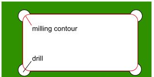
The outer of contour could be 90°or round according to customers’ specification but the inner corner of the profile has at least the radius of the milling cutter
Generally, the corner of the rectangle is round, to maintain a precise rectangular section, the corresponding milled part should also be drilled at the corners
PCB breakaway and outline are normally milled. Whereas, there are some rules:
1. Generally, it is no extra charge for milling.
2. It is necessary to avoid copper(durability of the circuit board, risk of injury).
3. To prevent the problem of the measurement and dimension, the inner and outer outline of the board should be indicated with a line width of 1μm.
Advantages
PCB milling has advantages for both prototyping and some special PCB designs. Probably the biggest benefit is that one doesn't have to use chemicals to produce PCBs.
When creating a prototype, outsourcing a board takes time. The alternative is to make a PCB in-house. Using the wet process, in-house production presents problems with chemicals and disposing thereof. High-resolution boards using the wet process are hard to achieve and still, when done, one has to drill and eventually cut out the PCB from the base material.
CNC machine prototyping can provide a fast-turnaround board production process without the need for wet processing. If a CNC machine is already used for drilling, this single machine could carry out both parts of the process, drilling, and milling. A CNC machine is used to process drilling, milling, and cutting.
Many boards that are simple for milling would be very difficult to process by wet etching and manual drilling afterward in a laboratory environment without using top of the line systems that usually cost multiple times more than CNC milling machines.
In mass production, milling is unlikely to replace etching although the use of CNC is already standard practice for drilling the boards.
Products categories
-
Factory Cheap Electronic Smt Fr4 Rigid Metal Pc...
-
Special Design for Shenzhen Multilayer Gold Fin...
-
Low MOQ for 16 Lines Electronic 1-58 Layers Bar...
-
Board2-300x300.jpg)
Europe style for OEM service heavy copper PCB b...
-
Quots for Copper Clad Pcb Board Pcb Pcb In Pcba...
-
Good User Reputation for Turnkey Service Electr...


Board2-300x300.jpg)

