
The classification of HDI products is determined by the recent development of HDI boards and the strong demand for their products.
Mobile companies and their suppliers have led the way in setting standards. In turn, the demand for products has led to a change in the technical limitations of mass production and a more affordable price.
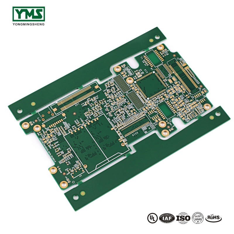
HDI technologies can be divided into several types of technologies.
The main drivers of HDI products are mobile communications products, high-end computer products and packaging substrates. The technical requirements of these products are completely different. Therefore, there are not one HDI technology, but several, which are classified as follows:
1. Miniaturized HDI products
Miniaturization of HDI products originally meant a reduction in the size and weight of the finished product through its own wiring density design and the use of new high-density devices such as uBGA. In most cases, the product continues to improve even as prices remain stable or decline. The interconnect is mainly composed of 6 or 8 layers.
2. High-density substrate HDI products
HDI board of high-density substrate are mainly concentrated in 4 or 6 layers, interlayer interconnection is realized by embedded holes, in which at least two layers have microholes. Its purpose is to meet the increasing demand of flip chip high density I/O number. The technology will soon be integrated with the HDI to achieve miniaturization.
This technology is suitable for flip chip or bunding substrate. The microporous process provides sufficient spacing for high density flip chip, even for HDI products with 2+2 structure.
3. High level HDI products
High-rise HDI board are usually conventional multilayer boards with laser drilling from layer 1 to layer 2 or layer 1 to layer 3. It is another characteristic to use the necessary sequence lamination process to make microholes in glass reinforced materials. The purpose of this technique is to leave enough element space to ensure the required impedance level.
This technology is suitable for HDI boards with high I/O or fine spacing elements. The embedded hole process is not a necessary process in such products. The purpose of the micro-hole process is only to form the spacing between high-density devices.
We are committed to being a high quality HDI PCB manufacturer and service provider.
Post time: Sep-24-2019