
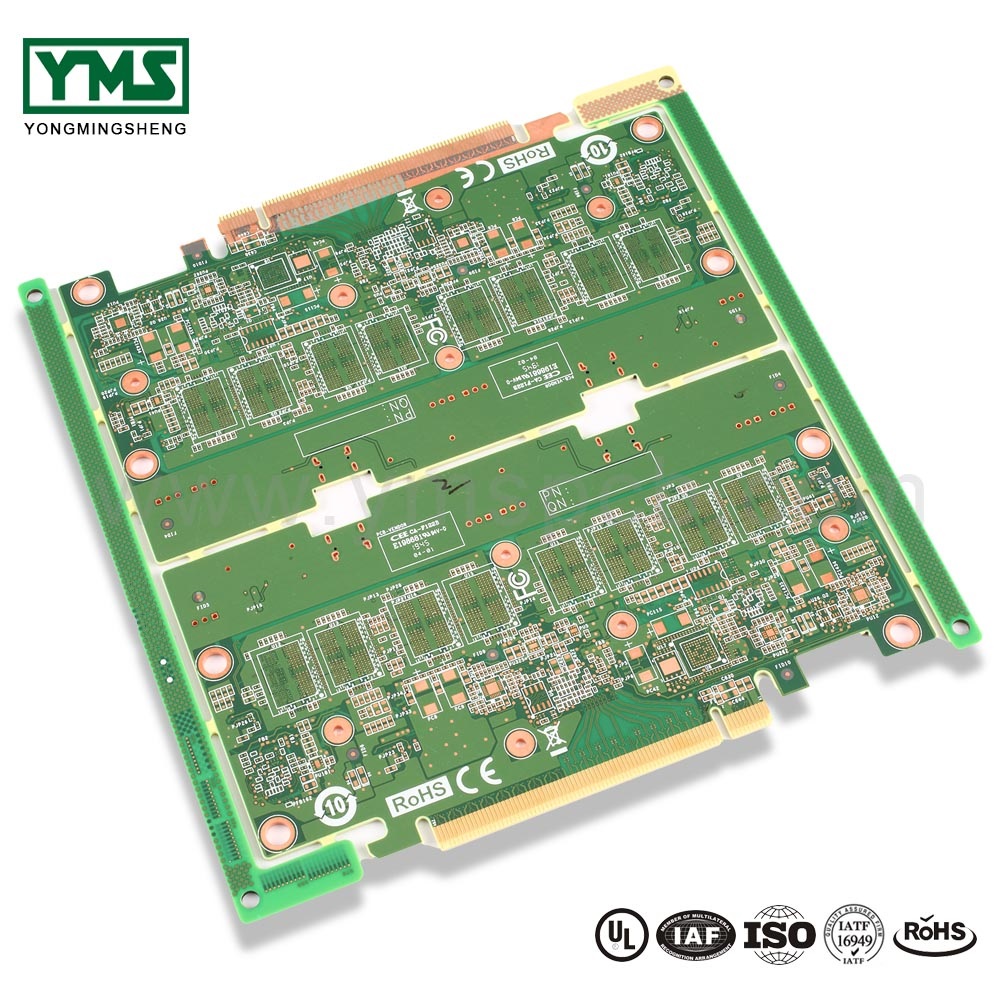
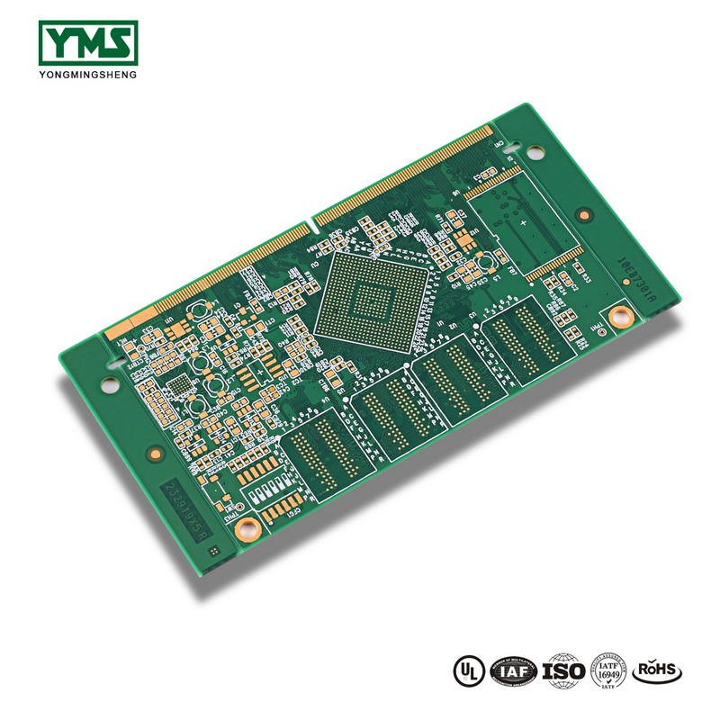
High Density Interconnector (HDI) is a kind of circuit board with high distribution density using microblind embedded hole technology. HDI board has inner circuit and outer circuit, which are connected by drilling and metallization.
HDI board is generally manufactured by the laminated method. The more times the laminated, the higher the technical level of the board. Ordinary HDI boards are basically one-time stacking, while high-order HDI adopts two-time or more stacking technology, and adopts advanced PCB technologies such as hole stacking, hole filling by electroplating and direct drilling by laser.
HDI pcb any layer hdi pcb high speed insertion loss test enepig
When PCB density increases by more than eight layers, the cost of manufacturing with HDI will be lower than the traditional complex pressing process. HDI board is beneficial to the use of advanced construction technology, and its electrical performance and signal accuracy are higher than traditional PCB. In addition, HDI board has better improvement for rf interference, electromagnetic interference, static electricity release, heat conduction, etc.
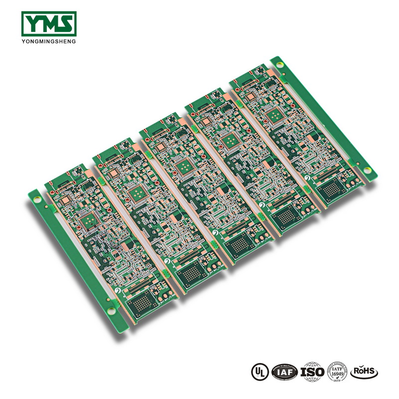
Electronic products continue to high-density, high-precision development, the so-called “high”, in addition to improving the performance of the machine, but also to reduce the size of the machine. High-density integration (HDI) technology enables the miniaturization of end product design while meeting higher standards of electronic performance and efficiency.
Many popular electronic products, such as mobile phones, digital cameras, laptops, and car electronics, use HDI boards. With the update of electronic products and market demand, the development of HDI board will be very rapid.
Introduction to common PCB
Printed Circuit Board, also known as Printed Circuit Board in Chinese, is an important electronic part, the support body of electronic components and the carrier for electrical connection of electronic components. Because it is made by electronic printing, it is called “printed” circuit board.
Its role is mainly electronic equipment adopts the PCB, due to the consistency of the same kind of PCB, so as to avoid the artificial connection error, and can realize automatic instrumentation or SMT electronic components, automatic soldering, automatic detection, ensure the quality of the electronic equipment, improve the labor productivity, reduce the cost, and easy maintenance.
Are PCB boards with blind holes called HDI boards
HDI board refers to high-density interconnection circuit board. The boards with blind hole electroplating and re-pressing are all HDI boards, which can be divided into 1-step, 2-step, 3-step, 4-step and 5-step HDI. For example, the main board of iPhone 6 is the 5-step HDI.
A simple buried hole is not necessarily an HDI.
HDI PCB 1-step and 2-step and 3-step how to distinguish
The 1-step is relatively simple, and the process and process are easy to control.
The 2-step is starting to get tricky, one is the counterpoint problem, one is the perforation problem and the copper plating problem. There are a variety of 2-step designs. One is the staggered position of each order. When the sub-adjacent layer needs to be connected with the intermediate layer through a wire, it is equivalent to two first-order HDI.
The second is that the two first-order holes overlap, and the second order is achieved by superposition. The processing is similar to the two first-order holes, but there are many technological points to be specially controlled, which is mentioned above.
The 3-step is to punch directly from the outer layer to the third layer (or n-2 layer), the process is a lot different from the front, the hole is more difficult.
The second analogy for the third order is.
The difference between HDI board and ordinary PCB
Common PCB board is fr-4 based, it is epoxy resin and electronic grade glass cloth pressed together. General traditional HDI, the most outside to use gum copper foil, because the laser drilling, can not get through the glass cloth, so the general use of non-glass fiber gum copper foil, but now the high-energy laser drill has been able to Pierce 1180 glass cloth. This is no different from ordinary materials.
We are committed to being a high quality HDI PCB manufacturers and service provider.
Post time: Sep-24-2019