
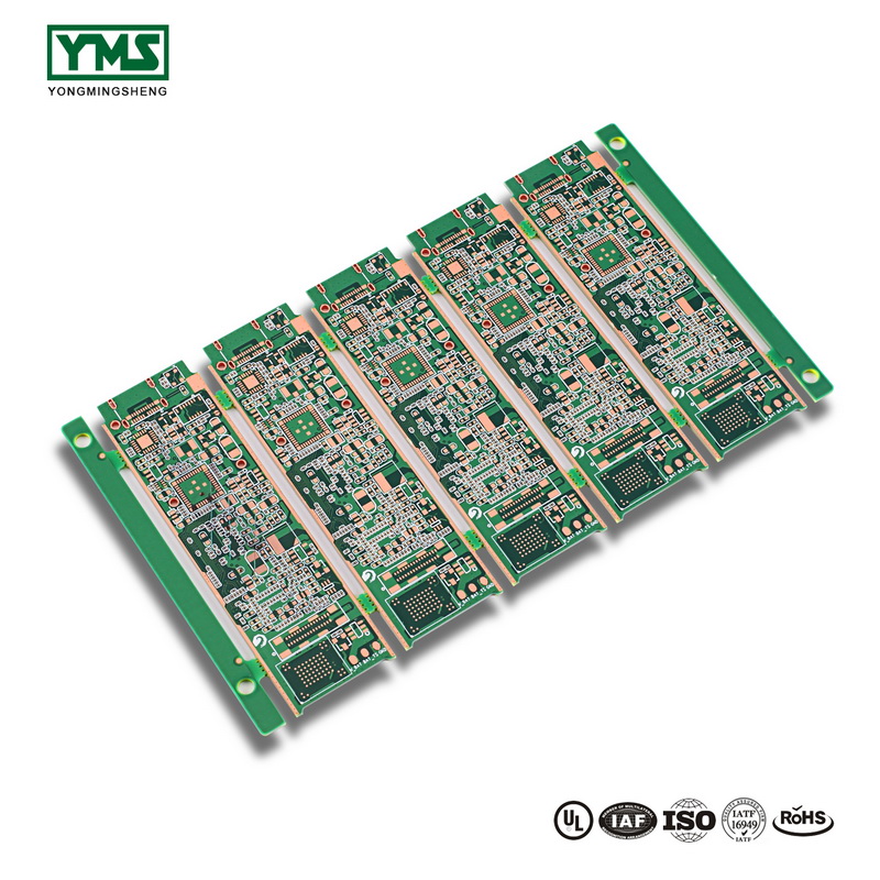
HDI, short for high-density interconnection, is the production of printed circuit boards, which use microblind burrow technology, a circuit board with a relatively high circuit distribution density.
HDI is a compact product designed for small volume users. It is designed to be modular and parallelizable, with a module capacity of 1000VA (height 1U), natural cooling, and can be placed directly into a 19 “rack, with a maximum of 6 modules parallel-connected.
HDI adopts full digital signal processing (DSP) technology and a number of proprietary technologies, with a full range of adaptive load capacity and strong short-term overload capacity, can not consider the load power factor and peak factor.
Application range of HDI board
The electronic design is not only improving the performance of the whole machine, but also reducing its size. From mobile phones to small, portable devices with smart weapons, “small” is a constant pursuit. High-density integration (HDI) technology enables the miniaturization of end product design while meeting higher standards of electronic performance and efficiency.
HDI is widely used in mobile phones, digital cameras, MP3, MP4, laptop computers, automotive electronics and other digital products, among which mobile phones are the most widely used. Generally, the HDI board is manufactured by build-up method. The more times of layering, the higher the technical level of the board.
Ordinary HDI boards are basically one-time stacking, while high-order HDI adopts two-time or more stacking technology, and adopts advanced PCB technologies such as hole stacking, hole filling by electroplating and direct drilling by laser.
HDI board is mainly used in 3G mobile phones, advanced digital cameras, IC board and so on.
HDI circuit advantages:
1. Reduce the cost of PCB: when the density of PCB increases more than eight layers, the cost of HDI manufacturing will be lower than the traditional complex pressing process.
2. Increase the line density: the interconnection of traditional circuit board and parts.
3. Conducive to the use of advanced construction technology.
4. Better electrical performance and signal correctness.
5. Better reliability.
6. Heat properties can be improved.
7. Improve rf interference/electromagnetic interference/electrostatic release (RFI/EMI/ESD).
8. Increase design efficiency.
We are committed to being a high quality HDI PCB manufacturer and service provider.
Post time: Sep-25-2019