
The reason of sticking tin on PCB gold finger
1, PCB board edge welt position is too close to the track edge, solder paste stick to the machine track.
2. The cleanliness of the printing press is poor. After each automatic cleaning, there will be some residues, some of which were just wiped to the goldfinger area, resulting in poor quality.
How to repair the sticking tin of PCB gold fingers
1, first with the absorption line to clean up the solder slag
2. Wipe the dirt with alcohol or water
3. Then use a 24-karat gold-plated pen.
How does PCB board gold finger clean better
1、 commonly used, is to use an eraser to wipe the golden finger, so that there is no chemical corrosion, recommended.
2、with anhydrous alcohol, dip in with medicaments cotton a little wipe, must be anhydrous.
3、with banana water, the same method as the second.
PCB gold finger window analysis!
What is PCB window opening?
Generally speaking, the conductor on the PCB is through the cover oil to prevent short circuit, open the window is to remove the paint layer on the conductor so that the conductor exposed convenient tin, that is, without anti-welding ink separated to achieve the purpose of "dew copper".
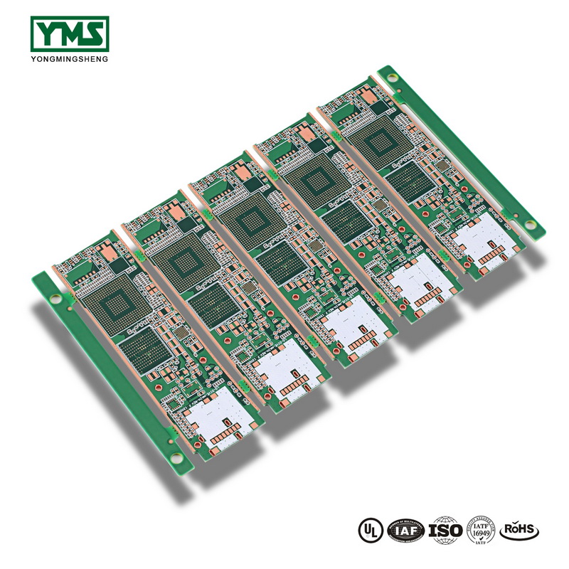
Among them, the most common PCB window opening is seen in golden finger, which is an electrical connection pin connected by PCB with other devices such as motherboard and chassis, and used for "plugging" on products. It is called "golden finger" because of a thin layer of gold plating on the nickel plating layer of copper foil.
We are familiar with the computer memory stick has a goldfinger structure, as anyone who has ever opened a computer knows, memory stick has one side of the goldfinger, above the goldfinger is the window, plug and play.
In general, the golden finger is made by "windowing" on the PCB process, that is, there is no anti-welding (green paint) between the pads, so as to avoid the anti-welding loss caused by long-term insertion and removal, which will affect the quality of the product itself.In addition, the window has a common function, in the late tin stamping can increase the thickness of copper foil to facilitate excessive current, which is more common in the power board and motor control board.
How to realize PCB window opening?Take Altium Designer 10 as an example, if you want to open a window on the Top Layer, you only need to place the same Line as the conductor on the Top Solder Layer. Similarly, if you want to open a window on the Bottom Layer, you only need to place Line on the Bottom Layer.
However, there are exceptions. If it is a general SMD(one of SMT components), this problem should be avoided. In PCB design, PAD spacing should be increased or PAD size should be reduced.
You May Like:
Post time: Sep-20-2019