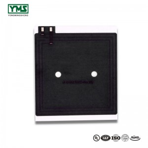
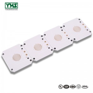
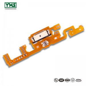
OEM China Multilayer HDI Back Drill PCB with Immersion Gold

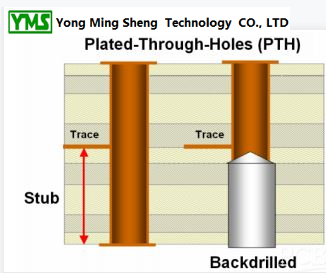
The backdrill process removes stubs from plated-through-holes (vias). Stubs are the unnecessary / unused portions of vias, which extend further than the last connected inner layer.
Stubs can lead to reflections, as well as disturbances of capacity, inductivity and impedance. This discontinuity errors become critical with increasing propagation speed.
Backplanes and thick Printed Circuit Boards in particular, can endure significant signal integrity disturbances through stubs. For High Frequency PCBs (e.g. with Impedance control), the application of backdrilling, as well as the application of blind and buried vias, can be part of the solution.
Backdrill can be applied to any type of circuit board where stubs cause signal integrity degradation, with minimal design and layout considerations. In contrast, when using blind vias, the aspect ratio has to be kept in mind.
Advantages:
• Reduced deterministic jitter
• Lower bit error rate (BER)
• Less signal attenuation with improved impedance matching
• Minimal design and layout impact
• Increased channel bandwidth
• Increased data rates
• Reduced EMI/EMC radiation from the stub end
• Reduced excitation of resonance modes
• Reduced via-to-via crosstalk
• Lower costs than sequential laminations
You May Like:
What is back drilling or controlled depth drilling in PCB?
High-speed PCB design faces many challenges in terms of retaining signal integrity which can be overcome through proper design and manufacturing practices. A via stub, a non-functional part of a via, causes significant signal integrity issues in high-speed design. Via stubs result in the reflection of signals from the stub end, and this reflection will interfere with the original signal. To counter this, back drilling is done, where most of the via stub is removed by re-drilling with a slightly larger sized drill bit.
Back drilling involves drilling a hole slightly larger in diameter than the PTH to remove the conductive via stub. The back drilled hole should bring down the stub length to 10 mils. If the stubs are greater than 10 mils, then signal reflections will be produced.
Why is back drilling required?
Back drilling or Controlled Depth Drilling (CDD) is a technique used to remove the unused portion (stub) of the copper barrel from a through-hole (via) in a printed circuit board. As these holes are back drilled to a predetermined, controlled depth, this type of drilling is also called controlled depth drilling. Ideally, the via stub left after back drilling should be lesser than 10 mil.