
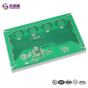
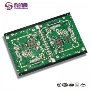
OEM Customized China Double Sided HASL Finish Fr4 Bare Making Machine PCB Board

We’ll make each individual effort to become exceptional and ideal, and speed up our steps for standing inside the rank of worldwide top-grade and high-tech enterprises for OEM Customized China Double Sided HASL Finish Fr4 Bare Making Machine PCB Board, Our tenet is “Reasonable costs, successful manufacturing time and finest service” We hope to cooperate with much more customers for mutual growth and rewards.
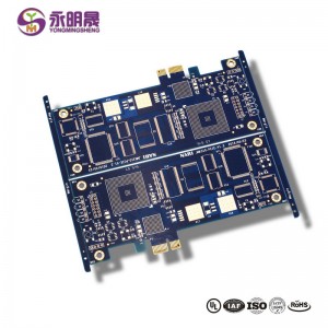
We’ll make each individual effort to become exceptional and ideal, and speed up our steps for standing inside the rank of worldwide top-grade and high-tech enterprises for China PCB Shenzhen Manufacturer, Printed Circuit Board, Welcome to visit our company, factory and our showroom where displays various products that will meet your expectation. Meanwhile, it is convenient to visit our website, and our sales staff will try their best to offer you the best service. Be sure to contact us if you have to have more information. Our aim is to help customers realize their goals. We’ve been making great efforts to achieve this win-win situation.
The production method of 2 Layer PCB is generally made by inner layer pattern first, and then made into single or double side substrate by printing etching method, which is incorporated into the specified layer, and then heated, pressurized and glued. As for the subsequent drilling, it is the same as the plating through hole method of double panel. These basic manufacturing methods have not changed much since the 1960s, but as materials and process techniques (e.g., pressing and bonding techniques, improvements to the glue residue produced by drilling, film) have matured, the properties attached to the multilayer have become more diverse.
You May Like:
1、Summary of matters needing attention in circuit board welding
Products categories
-
High Frequency PCBs manufacturing PTFE and FR4 ...
-
Online Exporter China 35um Copper Thickness Bar...
-
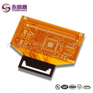
Flexible Circuit Board Supplier-Fast Delivery |...
-
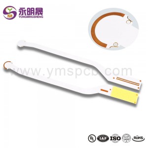
2layer Cem-3 Stiffener Flex PCB Manufacturer | ...
-
High Tg material PCB 6 Layer High Tg Board| YMS...
-
Board5-300x300.jpg)
Professional Design Heavy Copper Double Sided P...


Board5-300x300.jpg)