
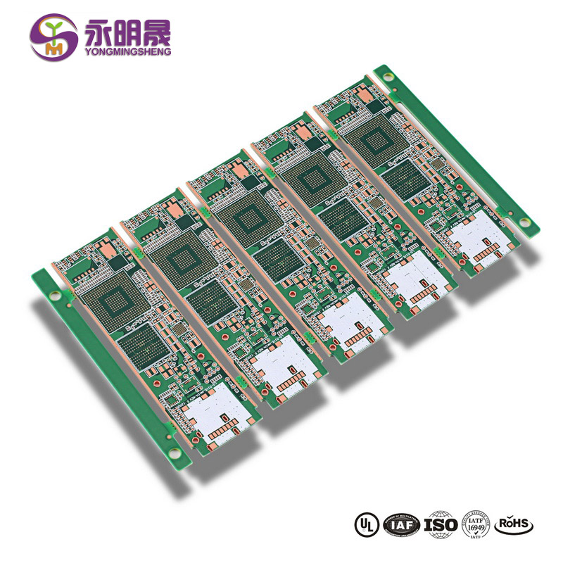
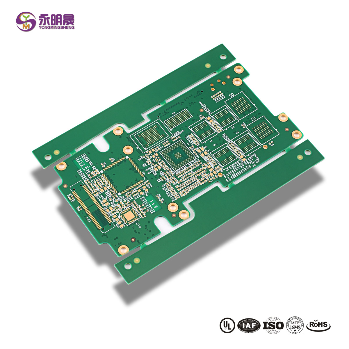
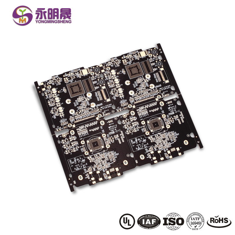
HDI PCB
YMSPCB: Your Leading HDI PCB Supplier in China
As for your best partner for HDIPCB. we offer you a better solution for your HD1 PCB design. Our CAM engineering department could provide some good suggestions when your project has some design problems so that it will save you some cost.
we offer different types of PCBs such as 1+n+1 2+nt2. 3+n+3.and anv aver HD1 PCB.YMSpcb also offers a wide range of raw materials for your choice including Shengyi, KB, NanYa, ITEO, FR408, Rogers, Taconic, Arlon, and Nelco laminates.
We assure you that meet every detailed requirement of the Gerber file. if there is any design issue, we will inform you immediately by email prior to starting the manufacturing
HD1 PCB assembly is one of our areas of expertise. This information is provided to you so that you can learn more about our product offerings.
Custom HDI PCB
We put at your disposal our know-how for the most complex printed circuit designs with parameters or characteristics so special that they require the personal assistance of our team. We will provvide customized solutions that meet your needs simply by sending us your files by e-mail.
HDI PCB: The Ultimate FAQ Guide
HDI PCBs are powered by smaller vias, lines, and spaces. HDI PCBs are very lightweight, which goes: hand in hand with their downsizing.
On the other hand, features high-frequency transmission, control redundant radiation, and impedance control on PCB. The board density is high because of the miniaturization of the board
Micro vias, blind and buried vias, high performance, thin materials, and tiny lines are all features of printed circuit boards.HDI PCBs are powered by smaller vias, lines, and spaces. HDI PCBs are very lightweight, which goes hand in hand with their downsizing.
On the other hand, features high-frequency transmission, control redundant radiation, and impedance control on PCB. The board density is high because of the miniaturization of the board
Micro vias, blind and buried vias, high performance, thin materials, and tiny lines are all features of printed circuit boards.
Engineers must have a thorough understanding of the design and HDI PCB manufacturing processes. The microchips on the HDl printed circuit boards need special attention throughout the assembly process, as well as superior soldering techniques
The smaller sizes and weights ft the HDI PCBs in compact designs like portable computers, mobilephones, etc. Because of their smaller size, HDI PCBs are also less prone to cracks.
As we mentioned before, the HDI printed circuit boards are not the same as the typical PCBs, so you need to keep some facts while doing the HDI PCB design.
As a PCB designer, you should follow the following HDI PCB design guidelines.
Keep Space Priority in Mind
As the main objective of HDI PCBs is the density of the components, you must think about as many components as you can implement, Along with a lot of components, you must consider the future maintenance of the PCBs.
On the other hand, ensure the proper spacing among the components. Keep in mind that you must give importance to the via diameter, trace width, and pad diameter for the flawless HDI manufacturing process.
Understanding Via Essence
Vias are one of the most important factors in HDI PCB design, You must understand the via implications on your HDI circuit board design.
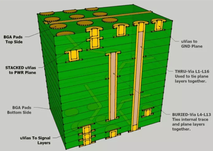
Vias are holes in PCBs that connect the different layers in the PCB electrically. Using multiple layers and connecting them using vias reduces the PCB size.
As the main goal of HDl circuit boards is to reduce their size, vias are one of the most important factors for them. Visas are available in different types. Through-Hole Vias
lt passes through the whole PCB, from its surface layer to its bottom layer, and is known as through-hole via. By this point, they connect all of the layers of the printed circuit board. But. through-hole vias take more space and reduce space for components.
Blind Vias
Blind vias just connect the external layers of the PCBs with the internal layers. No need to drill the entire PCBs.
Buried Vias
Buried vias are used to connect the internal layers of the PCBs. Buried vias are not visible from the outside of the PCBs.
Microvia
Microvia is the smallest via size less than 6 mils. You need to use laser drills to form micro vias.
So, basically, micro vias are used in HDl circuit boards.
lt is because of its size. As you need component density and no way to waste space in HDI PCBs, it is wise to replace other common vias with micro vias. Also, micro vias don't create thermal expansion issues (CTE) as they have short barrels.
Depending on the design requirements and application, HDI PCBs are formed in different structures.
Let's have a look at a quick illustration of the HDI PCB construction in the next section.
1+N+1: The Simplest Structure
A"build-up" high-density connectivity layer is included in the 1+N+1 construction. In this configuration, there are fewer l/O counts available in BGA.
Micro vias, tiny lines, and registration technologies are all found in 1+N+1. These can produce a 0.4 mm ball pitch. Furthermore, the mounting stability and reliability of this design are exceptional. it also has a copper-filled vial in it.
This HDl structure is used in cell phones, GPS devices, memory cards, and other devices.
2+N+2: Moderate Complex HDIStructure
Basically, there are at least two connecting layers in this architecture. More layers of build-up might also be employed. Micro vias are utilized in various PCB layers, and they may be stacked or staggered in their placement.
As HDl printed circuit boards are designed with complex and highly advanced technology, high-end electronics use them.
The devices that use HDl circuit boards are highly complicated and generate excellent performance. The following are the applications mentioned of HDI PCBs according to industries.
Consumer electronics: smartphones, touch screens, laptops, digital cameras, 4,5 G network communications, military communication systems, etc.
Aerospace industries: use HDl circuit boards where decreased weight is a concern.
The automotive industry: is becoming more computerized and highly microprocessor-dependent. Smart cars are increasing the use of auto-control GPS, rear cameras, backup sensors, etc through PCBs.
Medical equipment: such as monitoring, imaging, surgical, laboratory devices, etc., are using HDl
Industrial automation and loT are becoming more popular. HDI PCBs are the common power providers of them.
HDI PCBs are capable of doing a lot with a little size. The fundamental objective is to make electronics smaller.
As a result, HDI circuit boards are compact, take up less space and perform better. HDI printed circuit boards enable the deployment of more transistors by reducing the distance between the trace space. In addition,HDI uses less electricity and provides better signal transmission. Aside from these, the following advantages are found in using HDI PCBs.
HDl is cost-effective when you properly plan and implement the design manufacturing are advantageous with faster production.
Micro vias are used in HDI printed circuit boards. they are reliable, dependable, less space-consuming, and allow more space for the components.
These types of materials are from the FR4 family. They are loss-prone to the dielectric. The regular speed materials are used in a particular range of bandwidth. Isola 370HR is an example of this material family.
Surface mount technology is a component placement technology on PCBs. lt allows mounting components on the PCB without drilling the PCB for components.
As SMT components don't need any drilling, they occupy smaller space. So, the components could be mounted in a compact space. For this reason, SMT is used in higher-density designs like HDl
There are many advantages of SMT technology. Theta er as follows.
A smaller and more compact PCB design is possible with SMT technology as you can mount more components in a compact space.
SMT mounting process is faster and leaves fewer leads and leftovers.
High-frequency PCB,fast signaling, etc, are created with SMT.
You can mount the components on both sides of PCBs.
SMT components create less electromagnetic interference.
As the components are small and lightweight, the weight of the PCBs is reduced.
Drilling holes are one of the most significant features of high-density interconnect (HDl) printed circuit boards. Because of the smaller and more compact design, it is not envisaged that typical holes will be present.
For HDI PCBs, you must utilize laser drilling or laser direct imaging as opposed to conventional methods.
Because conventional drilling will result in larger holes, which are not acceptable with technology, traditional drilling is not recommended. ln order to reduce the amount of wasted space in HDl, micro vias are used.
The length of the hole will rise in proportion to the increase in the number of layers. The maximum diameter of micro vias in HDI PCBs, on the other hand, is 50 um.
Be precise for component selection. HDl boards need a high pin count SMD and BGA that is less than 0.65 mm. You need to select them wisely as they impact the via type, trace width, and HDPCB stack up.
You need to use micro vias in HDI boards. This will allow you to get double spaces than through-hole or other vias.
it is necessary to use materials that are both effective and efficient. lt is critical for the manufacturability of products.
To get a plain PCB surface, you should fill the vias' holes.
Iry to select materials for all layers with the same CTE rate. Keep an eye on thermal management, Make sure you properly design and organize layers that can properly dissipate the excessive heat.
The layout of an HDl circuit board ensures the component and wire density along with ensuring the smallest possible size of the PCB.
The layout of the HDl board means the techniques to keep the trace width under 8 mils. The HDayout consists of the following things. Vias Sized Small
Basically, micro vias are used in HDI circuit boards. They consume smaller space that ensures more space for the component placement, The size of the PCB becomes compact due to this reason.
Traces with Thinner State
Connecting circuits and vias is accomplished by the use of fine traces. Additionally, they are available as in-pad vias. Thinner traces are responsible for creating increased trace density in the background.
Layer Count Remains Higher
The HDI PCB layout contains a higher layer count, Counting 20 layers is a normal fact in HDI boards.
Low Signal Level
HDl circuit boards are not used for higher current flow applications. The lower signal level is another fact in the HDI circuit board layout.
The HDl board's sequential stack-up aids in the layer-by-layer construction of the HDI PCB stackup.Although this technology is used to create multilayer printed circuit boards, it is especially important for high-density to interconnect (HDl) printed circuit boards.
The sequential buildup is as follows.
Photoresist Deposition and Exposure
You will be able to specify the etching region of the PCB using this procedure. lt will result in a pattern of conductors on the PCB laminate as a consequence of this.
Etching and Cleaning
Etch the traces with ferric chloride to make them more visible. After the etching process is completed, clean the surface of the PCBs. ensure that no photoresist is left on the surface
Via formation and Drilling
Drill the board using a laser direct imaging method to add micro vias. The remaining via holes are then chemically removed. Metallization Of Vias
After you have established and structured the vias, you must metalize them in order to allow connections between the layers to be made.
Stack-up
The inner layers are now stacked in preparation for the outer layer processing.
Metalization is the process of depositing a thin copper coating on a dielectric surface. The metalized dielectric surface is located inside the vias that are drilled into the PCB lavers in order to link them together.
When sequential construction is being carried out, it is essential to guarantee that each layer is metalized to the highest possible standard. As a side note, you should be careful about the cracking of the vias and internal body of the printed circuit boards.
However, four types of PCB metallization are there. They are conventional electroless and electroplating copper, conductive pastes, conventional conductive graphite, and fully and semi-additive electroless copper. As a side note, you should be careful about the cracking of the vias and internal body of the printed circuit boards.
However, four types of PCB metallization are there. They are conventional electroless and electroplating copper, conductive pastes, conventional conductive graphite, and fully and semi-additive electroless copper.
The HDI PCB stackup is the organizing of the layers one by one. The number of layers or stack up could be determined based on the needs. However, this could be 8 layers to 40 layers or more.
But the exact numbers of layers are dependent on the density of traces. The multilayer stack up helps you to reduce the PCB sizes. lt also reduces the cost of manufacturing.
By the way, to determine the layer count of your HDI PCB, you need to determine the trace sizing and nets per layer. After determining them, you can calculate the required layer stackup of your HDI circuit board.
It is true that HDl circuit design takes more effort due to its complexity. For this, you must choose the right HDI PCB manufacturer for manufacturing this complex PCB to be done.
Because of the intricate nature of the design, the maker must possess exceptional qualifications.
When looking for a manufacturer, you should look for the following characteristics.
To make HDI PCBs, a manufacturer must be equipped with cutting-edge technology and
production capabilities.
They must have a quality management system that is integrated across the organization.
Must hold IPC certification.
Must have extensive experience in the field.
The office staff must be highly trained and skilled.
The mentioned criteria will make a manufacturer fit for manufacturing the complex HDl printed circuit boards.
If you cannot find an answer to your question in our FAQ, you can always contact us and we will be with you shortly.