
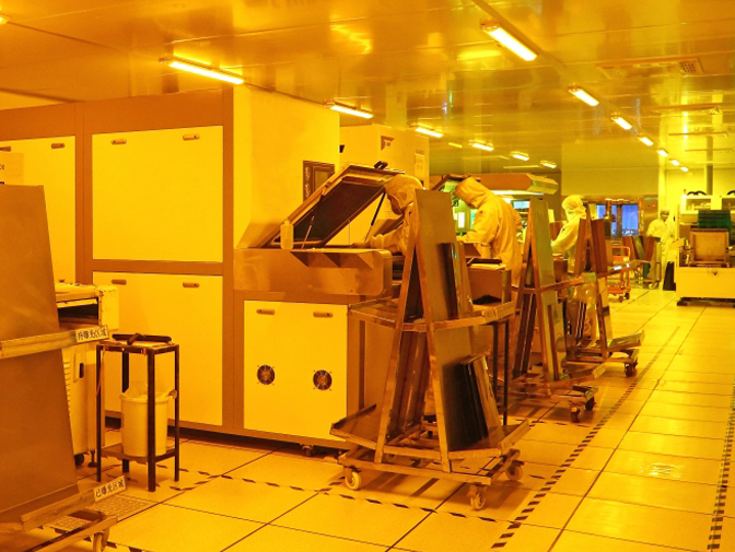
Best Multilayer Pcb Manufacturer,factory In China
YMSPCB is used to manufacture and assemble multilayer PCBS at favorable prices
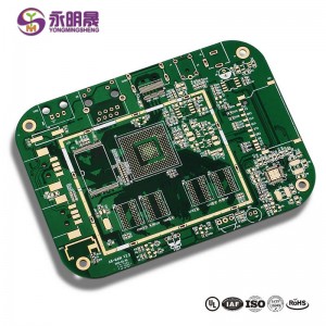
Multilayer PCB Manufacturer
As technology continues to advance and the number of multilayer PCBS in use is expected to expand, your company needs to invest in these trends and increase your focus on multilayer solutions. This increased focus should include working with quality multilayer PCB manufacturers and assemblers. With a solution like this, your company will be fully prepared to handle any multi-layer PCB project you encounter. YMSPCB can help you achieve your goals.
YMSPCB is a custom PCB solution provider that provides PCB manufacturing and assembly services to companies around the world. We help companies from parts procurement to testing while always meeting IPC Class 3, RoHS and ISO9001:2008 standards. We will be with you every step of the way through the entire process of producing multilayer PCBS and provide expertise and advice when needed. Our experienced team has produced thousands of multilayer PCBS that vary in design and complexity. No matter how complex the design or how extensive your needs are, YMSPCB can help.
To learn more about YMSPCB and our manufacturing and assembly capabilities, explore our manufacturing and assembly capabilities by clicking the following page links. If you would like more information on how we can help you individually, please feel free to contact us directly with a question.
Best Multilayer Pcb Manufacturer
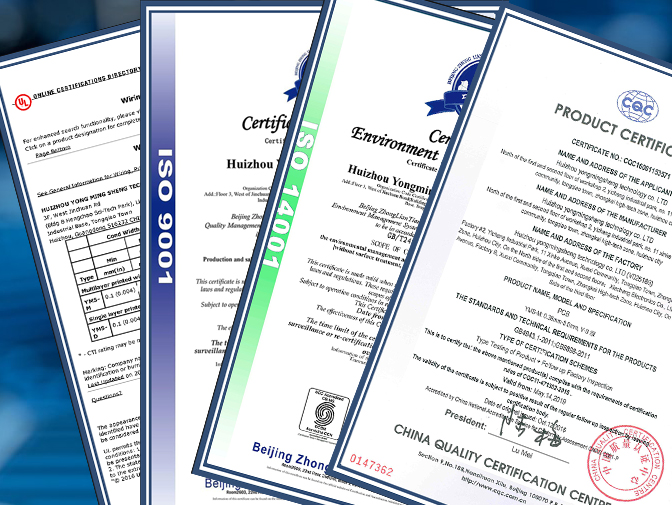
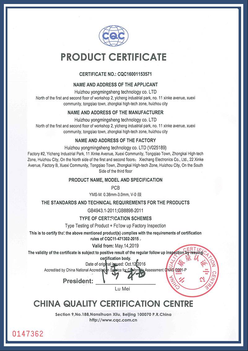
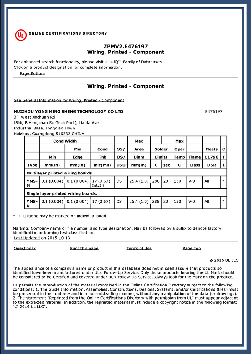
Certificates From PCB Manufacturer And Factory
The certificates and honors gained by YMS in the last 10 years are as follows:
ISO9001 certificate (In 2015 ),
UL certificate (In 2015 ),
CQC certificate No. 16001153571
Advanced technology enterprise (In 2018),
New and high technology enterprise(In 2018),
ISO14001 certificate( in 2015 ),
IATF16949 quality system(in 2019 ) .


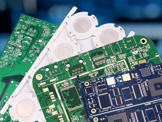
Choose Your Multilayer PCBs
A Multilayer PCB is a printed circuit board that has more than 2 layers, Unlike a Double-Sided PCB which only has two conductive layers of material, all multilayer PCBs must have at least three layers of conductive material which are buried in the center of the material.
YMSPCB has been producing Multilayer PCBs for over 10 years. Over the years, we have seen all types of multilayer constructions from various industries, answered all types of multilayer questions, and solved all types of problems with multilayer PCBs.
Why Choose YMCPCB
As a professional multilayer PCB manufacturer and factory, our positioning is to be a customer’s technical, production, after-sales, R&D team, quickly and professionally provide various multilayer pcb manufacturing solutions to solve various problems encountered by customers. Our customers only need to do a good job in the sales of multilayer pcbs, the other things such as controlling cost, PCB design & solutions, and after-sales, we will help customers deal with it in order to maximize customer benefits.
Steps Used in the Manufacturing of Multilayer PCB
Plan the layout PCB design following all the requirements and encode it. By doing this, you are making sure that the different aspects and parts of the designs are error-free. A completed PCB design is then ready for fabrication building.
As soon as the check completion has been finalized on the design, then it can be printed. You punch the registration hole to serve as a guide for aligning the films as you continue with the process.
This step is the first while making the inner layer of the PCB. You print the multilayer PCB design; then copper is re-bonded to the lamine piece that serves as the PCB structure.
Copper that photoresist does not cover is removed with a strong and effective chemical. As soon as it is removed, it leaves just the needed copper for your PCB.
Once the layers are free from defects, then you can fuse them. You can achieve this process in two spes, which include the lay-up and the laminating step.
Before you drill, the drill spot is located with an x-ray machine. This helps in securing the PCB stack.
This process helps in fusing the different PCB layers making use of a chemical.
By doing this you are guarding the copper found on the outer layer by applying the photoresist.
To protect the copper during the process, a tin guard is utilized. This gets rid of unwanted copper. This also ensures properly established PCB connections.
After cleaning the PCB panels, you apply an ink epoxy with a solder mask.
PCB plating is done to make sure that the soldering of the components can be achieved. The process of screening points all the important information on the PCB.
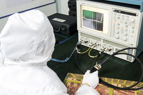
To ensure functionality, the technician carries out tests on several areas of the PCB.
According to the requirements of the customer, different PCBs are cut from the initial panel. Then the inspection of the board is done, and the errors rectified before it is sent for delivery.
Processes for Manufacturing Multilayer PCBs
Due to the sheer demand for multilayer PCBs for use in technology devices, healthcare equipment, military use, and even such consumer products as smart televisions and home monitoring equipment, most competitive manufacturers have positioned themselves to respond to the need for these boards. There remains a mix of capabilities among fabricators related to volume production capabilities, and the number of PCB layers that can be produced.
Manufacturing of multilayer PCBs involves a process of combining alternating layers of prepreg and core materials into a single unit, utilizing heat and high pressure to ensure uniform encapsulation of conductors, elimination of air between layers, and proper curing of adhesives that bind the layers together.
Due to the multiple layers of material, execution of drill holes among layers must be carefully observed and registered. It’s important for successful manufacturing of multilayer PCBs that engineers incorporate symmetrical layout across layers, to help avoid twisting or bow in the materials when heat and pressure are applied.
When sourcing a fabricator for multilayer PCBs, it is critically important to acquire the manufacture’s capabilities and standard tolerances for these complex boards, and utilize design for manufacturing (DFM) techniques to accommodate those standards. This goes a long way toward building confidence that the result will meet all functional, reliability, and performance expectations.
Advantages & Disadvantages
Advantages of multilayer PCBs
1. Small size: The most prominent and acclaimed advantage of multilayer PCBS is their size. Due to its layered design, multilayer PCBS are much smaller in volume than other PCBS with the same function. This has resulted in significant benefits for modern electronics, adapting to the current trend towards smaller, more compact but more powerful, like smartphones, laptops, tablets and wearables.
2. Lightweight construction: The smaller the PCB, the lighter the weight, which is beneficial to the design, especially when the multiple separate interconnectors required for single and double layer PCBS are eliminated. And especially convenient for modern electronic product design, just adapt to their mobility bias.
3. High Quality: Because of the amount of work and planning that must go into creating multilayer PCBS, these types of PCBS tend to outperform single and double layer PCBS in quality. As a result, they also tend to be more reliable.
4. Durability: Multilayer PCB materials tend to be durable because they must not only bear their own weight, but also be able to withstand the heat and pressure used to bond them together. In addition, multilayer PCBs have multiple insulation layers between the circuit layers and use prepreg adhesives and protective materials, which also make them more durable.
5. Flexibility: While this does not apply to all multilayer PCB components, some do use flexible construction techniques, resulting in flexible multilayer PCBS. This may be a desirable feature for applications where slight bending and bending may occur on a semi-regular basis.
6. Single connection point: Multilayer PCBS are designed to work as a single unit rather than in series with other PCB components. As a result, they have only one connection point, rather than the multiple connection points required to use multiple single-layer PCBS. It turns out that this is also beneficial in electronics designs, as they only need to include a single connection point in the final product. This is especially beneficial for small electronics and gadgets designed to minimize size and weight.
Disadvantages of multilayer PCBs
1. Higher cost: Multilayer PCBS are significantly more expensive than single and double layer PCBS at every stage of the manufacturing process. The design phase, which takes a lot of time to resolve any potential problems. The production stage requires very expensive equipment and highly complex manufacturing processes, which cost a lot of time and labor of assemblers. In addition, any errors in the manufacturing or assembly process are difficult to rework, and scrapping adds additional labor costs or scrap expenses.
2. Limited availability: Multi-layer PCB production machines are not available to all PCB manufacturers because they have the money or need. This limits the number of PCB manufacturers that can produce multilayer PCBS for customers.
3. Need a skilled designer: As mentioned earlier, multi-layer PCBS require a lot of prior design. This can be problematic without prior experience. Multilayer boards need interlayer interconnection, but crosstalk and impedance problems must be alleviated at the same time. A problem in the design may cause the board not to work properly.
4. Production time: with the increase of complexity, the manufacturing requirements also increase, which will lead to the turnover rate of multi-layer PCB. Each circuit board takes a lot of time to produce, resulting in more labor costs. So the time between placing an order and receiving the product is longer, which can be a problem in some cases.
Multilayer PCB Application
The advantages and comparisons discussed above lead to the question: What is the use of multilayer PCBS in the real world? The answer is almost anything.
For many industries, multilayer PCB has become the first choice for various applications. Much of this preference stems from the continued push for mobility and functionality across all technologies. Multilayer PCBS are a logical step in this process, enabling greater functionality while reducing size. As a result, they have become fairly common and are used in many technologies, including:
1. Consumer electronics: Consumer electronics is a broad term used to cover a wide range of products used by the general public. This tends to include products for everyday use, such as smartphones and microwaves. These consumer electronics products increasingly use multi-layer PCBS. Why is that? Much of the answer lies in consumer trends. People in the modern world tend to prefer multi-functional gadgets and smart devices that are integrated into their lives. From universal remote controls to smartwatches, these types of devices are fairly common in the modern world. They also tend to use multi-layer PCBS to increase functionality and reduce size.
2. Computer electronics: Multilayer PCBS are used for everything from servers to motherboards, mainly because of their space-saving properties and high functionality. For these applications, performance is one of the most important characteristics of the PCB, while cost is relatively low on the priority list. Therefore, multilayer PCBS are an ideal solution for many technologies in the industry.
3. Telecommunications: Telecommunications equipment typically uses multilayer PCBS in many general applications, such as signal transmission, GPS, and satellite applications. The reasons are mainly due to their durability and functionality. PCBS for telecommunications applications are typically used in mobile devices or outdoor towers. In such applications, durability is essential while still maintaining a high level of functionality.
4. Industry: Multilayer PCBS are indeed proving to be more durable than several other options currently on the market, making them ideal for everyday applications where rough handling may occur. As a result, multilayer PCBS have become popular in a variety of industrial applications, the most notable of which is industrial control. From industrial computers to control systems, multilayer PCBS are used throughout manufacturing and industrial applications to run machinery and are favored for their durability as well as their small size and functionality.
5. Medical devices: Electronics are becoming an increasingly important part of the healthcare industry, playing a role in everything from treatment to diagnosis. Multilayer PCBS are particularly favored by the medical industry due to their small size, light weight, and impressive functionality compared to single-layer alternatives. These advantages have led to multilayer PCBS being used in modern X-ray devices, heart monitors, CAT scanning devices, and medical testing equipment, among others.
6. Military and Defense: Favored for their durability, functionality, and light weight, multilayer PCBS can be used in high-speed circuits, which are becoming an increasingly important priority in military applications. They are also favored due to the defense industry's growing preference for highly compact engineering designs, as the small size of multilayer PCBS provides more space for other components to perform existing functions.
7. Cars: In modern times, cars rely more and more on electronic components, especially with the rise of electric vehicles. From GPS and on-board computers to electronically controlled headlight switches and engine sensors, using the right kind of components is becoming increasingly important in car design. That's why many automakers are starting to favor multilayer PCBS over other alternatives. Although they are small and durable, multilayer PCBS are also highly functional and relatively heat resistant, making them ideal for the interior environment of a car.
8. Aerospace: Like cars, jets and rockets, in modern times there is a heavy reliance on electronic devices, all of which must be very precise. From computers used on the ground to those in the cockpit, aeronautical PCB applications must be reliable and able to handle the stresses of atmospheric travel while making enough room for the rest of the equipment around them. In this case, multilayer PCBS provide an ideal solution, with plenty of protective layers to prevent heat and external stresses from damaging the connection, and are capable of being made of flexible materials. Their higher quality and functionality also contribute to this utility in the aerospace industry, as aerospace companies prefer to use the best materials to keep their personnel and equipment safe.
9. And more! Multilayer PCBS are used in a variety of other industries, including the scientific research industry and even home appliances and security. Multilayer PCBS are used for everything from alarm systems and fiber-optic sensors to atom-smasher and weather analysis equipment, taking advantage of the space and weight savings offered by this PCB format, as well as their enhanced features.
Frequently Asked Questions
The different materials utilized in manufacturing multilayer PCBs are boards, copper foil, resin system, substrate, vias, infused fiberglass sheet. Using an alternating sandwich, you can laminate these materials together.
All the planes of copper are etched and the plating through of all internal vias is done before the layers.
Multilayer PCBs come with lots of great benefits. Some of them include:
Higher assembly density
Provision of high speed and high capacity, as a result of their electrical properties
Weight reduction of devices
Elimination of connectors needed for multiple separate PCBs, thereby simplifying its construction.
Multilayer PCBs can be utilizes in many areas. Let’s consider some of them.
They are used in manufacturing CAT scan, heart monitors, and modern x-ray equipment.
Utilized in the production of high-speed circuits due to their functionality and durability
Used for headlight switches and onboard computers due to their high functionality and heat resistant ability
The running of machinery and industrial control system utilize them due to their small size and durability.
Consumer electronics such as microwaves and smartphones also make use of multilayer PCBs as a result of their small size and functionality.
Satellite applications, GPS, and signal information, also make use of multilayer PCBs
Used in the production of computer electronics that are utilized in M servers due to its performance and space-saving attributes.
You can identify a multilayer PCB through the following
How your electronic equipment operates briskly, as well as the ultimate board’s operational setting
The configuration, layer count, and the value of the board’s building also play a role in the identification
The board routing density
The operating capacity, speed, parameters, and functionality, distinguishes if the PCB is a multilayer one
They make use of simple production techniques, but still focusing on performance and quality.
Multilayer PCBs are usually difficult to style, in contrast to single-layer ones that have an easy production process
Single-layer PCBs are usually produced in large quantities and can also be ordered in bulk. This helps in reducing the price per board thereby ensuring that producing these devices are less expensive. For multilayer PCBs, producing them are usually tedious, and it may be difficult producing them in large qualities at once.
The components of the PCB include:
Led: The Led lets current flow in a direction
Capacitor: It is made up of an electrical charge
Transistor: Utilized in amplifying charge
Resistors: It helps in controlling the electric current when it passes through
Diode: Diodes allow the passing of current through one direction only
Battery: its gives the circuit its voltage
Hydraulic press: This ensures that metallic objects are transformed into metal sheets. This helps during thinning when making glass powder, as well as tablets making.
Prepreg: This is an important material utilized in multilayer boards. They help in holding the cores together. Prepregs are made up of fiberglass, which is impregnated with an epoxy-based material known as resin. Its layers are compact at a specific temperature. This helps in creating a specific board thickness.
Multilayer PCBs are widely used for the following reasons:
Multilayer PCBs are made utilizing high technology. This is why it is highly trusted due to the skills, processes, and designs required to manufacture it.
You can also attribute it to the fact that users always want something modern.
Its miniature size gives it its flexibility
It has a small size, and its performance is enhanced with its technology. Most users prefer a device having a smaller size
As a result of its less weight, it is portable enough and convenient for users. Users can easily carry the around, because they are not as bulky as some other smartphones.
Due to its fabrication process, users consider this PCB as one with high quality
It makes use of highly skilled professionals, modern technology, and high-quality materials.
Easy installation, which makes it widely used, hence there is no need getting the service outsourced
Multilayer PCBs come with a protective layer, which prevents damage from coming to it, as well as an increase in its durability
It is the most preferred due to its higher density, when compared to its counterparts. Users love devices that have a higher mass per volume degree, which should boast enough storage space.
Multilayer PCB come with some quality standards. They include
ISO 9001 makes sure that manufacturers meet the needs of customers within regulated and permitted requirements that concern a service or product.
ATF16949 is another quality standard requiring the manufacturers of electronics to assure the security and quality of automotive products. This helps in improving the reliability and performance of automotive components.
The UL listing service requires that manufacturers test their products thoroughly. This is to makes sure that specific requirements are met.
Yes, multilayer PCBs are categorized under HF PCBs. With multiple layers, the boards can have a great thermal coefficient and impedance control.
To be regarded among the high-frequency design applications, having a ground plane is very essential. Multilayer applications are utilized in high-frequency applications like smartphones and microwaves.
It can be manufactured in a PCB factory. The 4layers board generally uses a core with one copper foil on each sideand a 3layers board with one copper foil on one side. They must be pressed together.
The process cost difference between the two is that the four-layer board has one more copper foil and bonding layer. The cost difference is not significant. When the PCB factory makes a quote, they are generally quoted on an even number basis. Also, 3-4 layers are commonly quoted as a grade. (For example:If you design a 5-layer board, the other party will quote at the price of a 6layers board. That is to say, the price you design for 3 layers is the same as the price you design for 4 layers.)
In the PCB process technology, the four-layer PCB board is better controlled than the three-layer board, mainly in terms of symmetry. The warpage of the four-layer board can be controlled below 0.7% , but the size of the three-layer board is large. At that time, the warpage will exceed this standard, which will affect the reliability of the SMT assembly and the entire product. Therefore, the designer shouldnot design the odd-numbered layer board. Even if the odd-numbered layer is necessary, it will be designed as a fake even-numbered layer. That is to design 5 layers into 6 layersand 7 layers into 8 layers.
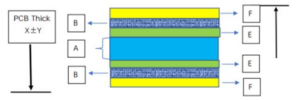
A: Thickness of inner layer
E: Thickness of inner copper foil
X: Finished board thickness
B: Thickness of PP sheet
F: Thickness of outer copper foil
Y: Finished PCB tolerance
1.Calculate the upper and lower limit of pressing:
Usually tin plate: upper limit -6MIL, lower limit-4MIL
Gold plate: upper limit -5MIL, lower limit -3MIL
For example, tin plate: upper limit=X+Y-6MIL lower limit=X-Y-4MIL
Calculate the median = (upper limit + lower limit)/2
≈A+the area of the second layer of copper foil%*E+the area of the third layer of copper foil%*E+B*2+F*2
The inner cutting material of the above conventional four-layer board is 0.4mm smaller than the finished board, using a single 2116 PP sheet to press. For special inner layer copper thickness and outer layer copper thickness that more than 1OZ, the copper thickness should be considered when choosing the inner layer material.
2.Calculate the pressing tolerance:
Upper limit = Finished board thickness + Finished on-line tolerance value-[Plating copper thickness, green oil character thickness
(Conventional 0.1MM)]-The theoretically calculated thickness after pressing
Lower limit = finished board thickness-finished product off-line tolerance value-[Electroplating copper thickness, green oil character thickness
(Regular 0.1MM)]-The theoretically calculated thickness after pressing
3.Commonly types of pp sheets

Generally, do not use two PP sheets with high resin content together. If the inner layer of copper is too small, please use PP sheets with high resin content. 1080 PP sheets have the highest density and low resin content. Do not press single sheets as much as possible. Only 2 sheets of 2116 and 7630 PP sheets can be pressed into thick copper plates above 2OZ. The layer cannot be pressed by a single sheet of PP. 7628 PP sheet can be pressed by a single sheet, 2 sheets, 3 sheets, or up to 4 sheets.
Explanation of theoretical thickness calculation of multilayer PCB board after pressing
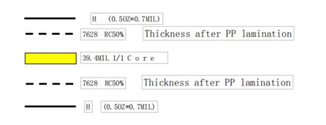
Thickness after PP lamination = 100% residual copper lamination thickness-inner copper thickness*(1-Remaining copper rate%)
As the name, multilayer PCBs are the combination of different multilayer circuits. A number of single-sided and double-sided PCBs are combined and separated by an insulating material (such as dielectric) to form a multilayer PCB of this complex design. It increases the number of layers and increases the area available for wiring.
The number of conductive layers between insulating materials is at least 3, and up to 100. We commonly have 4 to 12 layers, for example, smartphones are mostly 12 layers. The greater number of layers makes them suitable for the complexity of the application. Manufacturers prefer even layers because laminating an odd number of layers would make the circuit too complex and problematic.
Multilayer PCBs are generally rigid because it is difficult for flexible PCBS to reach multiple layers. Rigid multilayer PCBs need to be drilled to connect the different layers. Ordinary through-holes may waste space, so instead buried or blind through-holes are used, which only penetrate the necessary layers. Different layers can be classified into different planes, such as ground plane, power plane, and signal plane.
If you want to build a PCB, there are a variety of materials to choose from, such as special ceramics, epoxy plexiglass. The resin and binder materials then bond the components and the different layers together. Relaminating, performed at high temperatures and pressures, removes any trapped air between the layers and helps melt the different prepreg layers and core layers