
HDI Multilayer PCB-China PCB Manufacturer | YMSPCB

HDI is short for high density interconnect, and refers to the use of buried, blind and micro vias as well as any layer HDIs to create compact multilayer boards. Besides the obvious benefit in packing the same board functionality into a smaller footprint, HDI comes with a number of benefits when compared to traditional multilayer designs:
Advantage
Fewer layers
Improved signal integrity
Lower power consumption
Better electrical performance
At the heart of these benefits is the fact that reducing signal path throughout your board will naturally improve signal integrity and electrical performance, provided that you are able to properly account for EMI/EMC considerations.
Let’s take a closer look at the features that make HDI possible:
Function
Microvias are extremely small vias (often laser drilled) with an aspect ratio (depth to diameter) of 1:1
Blind vias connect an exterior layer to at least one interior layer without penetrating the entire board.
Buried vias connect one or more inner layers together without any connections to the exterior layers of a board.
Any layer HDI (or ELIC) refers to the use of stacked copper-filled microvias to connect multiple layers in a PCB.
Lamination & Materials For HDI Boards
Advanced multilayer technology allows for designers to sequentially add additional pairs of layers to form a multilayer PCB. The use of a laser drill to produce holes in the internal layers allows for plating, imaging and etching prior to pressing. This added process is known as sequential build up. SBU fabrication uses solid filled vias allowing for better thermal management, a stronger inter connect and increasing the board's reliability.
Resin coated copper was developed specifically to aide with poor hole quality, longer drill times and to allow for thinner PCBs. RCC has an ultra-low profile and ultra-thin copper foil that is anchored with minuscule nodules to the surface. This material is chemically treated and primed for the thinnest and finest line and spacing technology.
The application of dry resist to the laminate still uses heated roll method to apply the resist to core material. This older technology process, it is now recommended to preheat the material to a desired temperature prior to the lamination process for HDI printed circuit boards. The preheating of the material allows for better a steady application of the dry resist to the surface of the laminate, pulling less heat away from the hot rolls and allowing for consistent stable exit temperatures of the laminated product. Consistent entrance and exit temperatures lead to less air entrapment beneath the film; this is critical to the reproduction of fine lines and spacing.
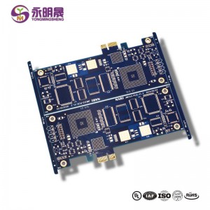
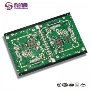
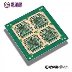
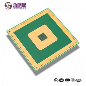
Huizhou Yongmingsheng Technology co., ltd. is one of the leading HDI Multilayer PCB manufacturers, factories & suppliers in China, accepting OEM, ODM orders. We have rich experiences in production & research development for different PCB types. We focus on advanced technology, strict manufacturing step, and a perfect QC system.
Learn more about YMS products
Read more news


What are the applications of multilayer PCBs?
Multi-layer PCBs are often used in various professional electronics such as computers, mobile phones, heart monitors and much more. Multi-layer PCB fabrication involves laminating more than two conductive layers together, with the number of layers varying depending on the application.
What is the difference between a single layer and a multilayer PCB?
Multi-layer PCBs feature numerous layers, whereas single-layer boards have only one layer of base material, commonly known as a substrate like single-sided PCBs, double-sided PCBs contain only one substrate layer. They are distinguished by the presence of a conductive metal layer on both sides of the substrate.
How many layers can a high-density multilayer PCB have?
The number of layers is referred to as the number of separate conductor patterns. It is usually even and includes the two outer layers. Most mainboards have between 4 and 8 layers, but high-density multilayer PCB with almost 100 layers can be made.
What is the location of my high density multilayer PCB?
More insulation layers are sandwiched between the PCB copper layers on multilayer printed circuit boards. By counting the number of insulation layers by eye, you can figure out how many PCB layers there are. Examine the via holes or blind vias to determine the number of PCB layers.
Difference of performance between a double-sided PCB and multilayer PCB
A high-density multilayer PCB can offer a 20-dB EMI/RFI performance advantage over a two-layer PCB. If manufacturing volumes are low, it makes more sense to start with a superior PCB rather than cutting corners and risk failing $25,000 to $50,000 tests.
Why SMD components are used in high-density multilayer PCB?
Initially, electronic components were only available in DIP packages, and PCB boards were large in size to allow for more PCB wiring and connections. However, as a result of nanotechnology research, SMD components have been introduced in high-density multilayer PCB.
Why high-density multilayer PCBs are introduced?
SMD components are extremely small components with the express objective of shrinking the overall size of electronic kits and circuits. As a result, when SMD components are utilised in PCBs, they are placed very close to one another, and in complicated designs, the tracing lines of connection wires are unable to pass.
So, to overcome this issue, high-density multilayer PCB invented, where connections are spread across several PCB boards called layers and these layers are laminated to maintain insulated from each other and glued together.
What is the worth of high-density interconnects?
High-density interconnects PCBs are an increasingly integral part of the PCB and electronics industries. Electronic components are becoming smaller and more lightweight but still demand ever-improving performance. To accommodate this, you need to pack more functionality into a smaller area.
What is the main issue in high-density PCBs?
Lack of space for the required number of vias is a common limiting problem in high-density multilayer PCB. Designers can progress onwards and upwards to multilayer boards to get over this issue.
Products categories
-
PCB bare board 4L Black Soldermask buried Hole ...
-

Wholesale Multi Layer PCB-PCB Manufacturer Chin...
-
China PCB 6Layer Gold Finger Blue Soldermask Bo...
-
High Tg material PCB 6 Layer High Tg Board| YMS...
-
Edge Plating PCB 10 Layer Board edge plating PC...
-
Thick Copper PCB 10 Layer (4OZ) High Tg Full B...


