
PCB bare board 4L Black Soldermask buried Hole PCB manufacturer | YMS PCB

Printed Circuit Board Introduction
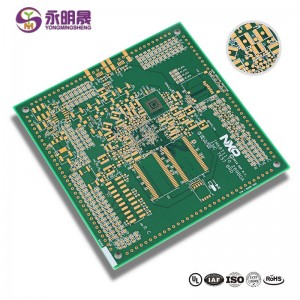
A printed circuit board (PCB) mechanically supports and electrically connects electrical or electronic components using conductive tracks, pads and other features etched from one or more sheet layers of copper laminated onto and/or between sheet layers of a non-conductive substrate. Components are generally soldered onto the PCB to both electrically connect and mechanically fasten them to it.PCBs can be single-sided (one copper layer), double-sided (two copper layers on both sides of one substrate layer), or multi-layer (outer and inner layers of copper, alternating with layers of substrate). Multi-layer PCBs allow for much higher component density, because circuit traces on the inner layers would otherwise take up surface space between components. The rise in popularity of multilayer PCBs with more than two, and especially with more than four, copper planes was concurrent with the adoption of surface mount technology.

YMS Normal PCB manufacturing capabilities:
| YMS Normal PCB manufacturing capabilities overview | ||
| Feature | capabilities | |
| Layer Count | 1-60L | |
| Available Normal PCB Technology | Through hole with Aspect Ratio 16:1 | |
| buried and blind via | ||
| Hybrid | High Frequency Material such as RO4350B and FR4 Mix etc. | |
| High Speed Material such as M7NE and FR4 Mix etc. | ||
| Material | CEM- | CEM-1;CEM-2;CEM-4;CEM-5.etc |
| FR4 | EM827, 370HR, S1000-2, IT180A, IT158, S1000 / S1155, R1566W, EM285, TU862HF,NP170G etc. | |
| High Speed | Megtron6, Megtron4, Megtron7,TU872SLK, FR408HR,N4000-13 Series,MW4000,MW2000,TU933 etc. | |
| High Frequency | Ro3003, Ro3006, Ro4350B, Ro4360G2, Ro4835, CLTE, Genclad, RF35, FastRise27 etc. | |
| Others | Polyimide, Tk, LCP, BT, C-ply, Fradflex, Omega , ZBC2000,PEEK,PTFE,ceramic-based etc. | |
| Thickness | 0.3mm-8mm | |
| Max.copper Thickness | 10OZ | |
| Minimum line Width and Space | 0.05mm/0.05mm(2mil/2mil) | |
| BGA PITCH | 0.35mm | |
| Min mechanical Drilled Size | 0.15mm(6mil) | |
| Aspect Ratio for through hole | 16:1 | |
| Surface Finish | HASL, Lead free HASL,ENIG,Immersion Tin, OSP, Immersion Silver, Gold Finger, Electroplating Hard Gold, Selective OSP,ENEPIG.etc. | |
| Via Fill Option | The via is plated and filled with either conductive or non-conductive epoxy then capped and plated over(VIPPO) | |
| Copper filled, silver filled | ||
| Registration | ±4mil | |
| Solder Mask | Green, Red, Yellow, Blue, White, Black, Purple, Matte Black, Matte green.etc. | |
Learn more about YMS products
Read more news

What is a blank PCB called?
A blank pcb board is a panel without any connections or components that is used to create a printed circuit board
What is unpopulated PCB?
An unpopulated board is a circuit board found inside a computer or hardware device with empty sockets for future upgrades or firmware updates
What are the 3 types of PCB?
1.FR-4 2.PTFE (Teflon)3.Metal core
Can we touch PCB with bare hands?
Absolutely not
Products categories
-
China PCB 6Layer Gold Finger Blue Soldermask Bo...
-
Multilayer PCB manufacturing from 4 to 60 Layer...
-

Wholesale Castellated Multilayer PCB from China...
-
FR4 Multilayer PCB-Chian Wholesale Supplier | Y...
-
HDI Multilayer PCB-China PCB Manufacturer | YMSPCB
-
Thick Copper PCB 10 Layer (4OZ) High Tg Full B...


