
If the PCB has more ground, there are SGND, AGND, GND, etc., depending on the position of the PCB surface, the main "ground" is used as the reference for independent copper coating, that is, the ground is connected together.
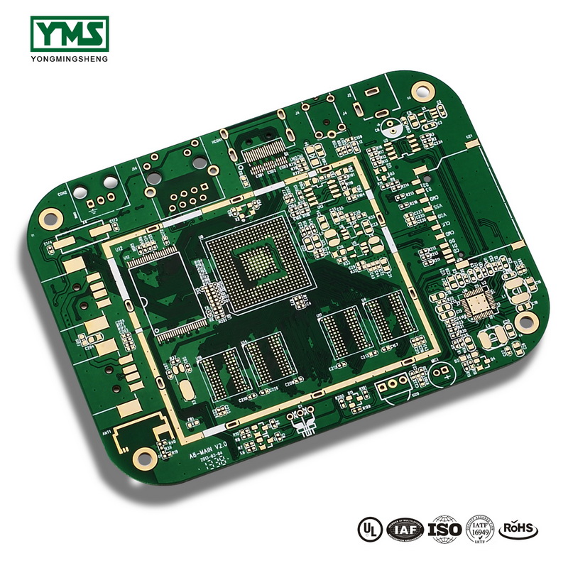
Copper Wrap Plating Structures
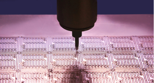
Filled via-in-pad structures require via holes be copper plated in order to route signals between layers in a multilayer PCB. This plating connects to other pads in via-in-pad structures, as well as directly to a trace using a small annular ring. These structures are indispensable, but they are known to have some reliability problems under repeated thermal cycling.
The IPC 6012E standards recently added a copper wrap plating requirement to via-in-pad structures. The filled copper plating should continue around the edge of the via hole and extend onto the annular ring surrounding the via pad. This requirement improves the reliability of the via plating and has the potential to reduce failures due to cracks, or due to the separation between surface features and the plated via hole.
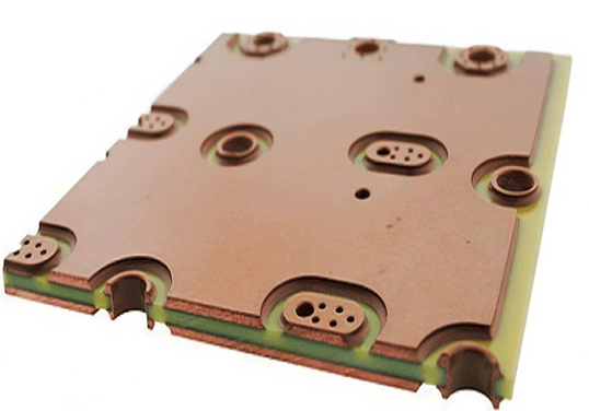
Filled copper wrap structures appear in two varieties. First, a continuous copper film can be applied to the inside of a via, which then wraps over the top and bottom layers at the ends of the via. This copper wrap plating then forms the via pad and trace leading to the via, creating a continuous copper structure.
Alternatively, the via can have its own separate pad formed around the ends of the via. This separate pad layer connects to traces or ground planes. The copper plating that fills the via then wraps over the top of this external pad, forming a butt joint between the copper fill plating and the via pad. Some bonding occurs between the fill plating and the via pad, but the two do not fuse together and do not form a single continuous structure.
There are several reasons for copper plating:
1. EMC. For a large area of ground or power copper, it will shield, and some special, such as PGND to protect.
2. PCB process requirements. Generally, in order to ensure the plating effect, or the laminate is not deformed, copper is laid for the PCB layer with less wiring.
3. Signal integrity requirements, give a high-frequency digital signal a complete return path, and reduce the wiring of the DC network. Of course, there are heat dissipation, special device installation requires copper plating and so on.
A major advantage of copper plating is to reduce the ground line impedance (the so-called anti-interference is also caused by a large part of the ground line impedance reduction). There are a lot of spike currents in the digital circuit, so it is more necessary to reduce the ground line impedance. It is generally believed that circuits composed entirely of digital devices should be grounded over a large area, and for analog circuits, the ground loop formed by copper plating may cause electromagnetic coupling interference to be inferior (except for high frequency circuits). Therefore, it is not a circuit that has to be copper (BTW: mesh copper is better than the whole block).
The significance of circuit copper plating:
1. copper and ground wire connected, this can reduce the loop area
2. the large area of copper plating is equivalent to reducing the resistance of the ground wire, reducing the pressure drop from these two points It is said that both digital ground and analog ground should be copper to increase the anti-interference ability, and at high frequencies, the digital ground and the analog ground should be separated to lay copper, and then connected by a single point, the single point can Use a wire to make a few turns on a magnetic ring and then connect. However, if the frequency is not too high, or the working conditions of the instrument are not bad, you can relax relatively. The crystal can be counted as a high-frequency source in the circuit. You can place copper around and ground the crystal case, which is better.
If you are interested in learning more about YMS PCB,contact us at any time.
Learn more about YMS products
Post time: Apr-08-2022