
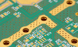
How Thick Is 1oz Copper?
In the printed circuit board industry, the most common way to express copper thickness on a PCB is in ounces (oz). Why use a unit of weight to specify a thickness? Great question! If 1oz (28.35 grams) of copper is flattened to evenly cover 1 square foot of surface area (0.093 square meter), the resulting thickness will be 1.37mils (0.0348mm). A conversion chart for different units of measure can be found below.
Copper Thickness Conversion Chart
|
oz |
1 |
1.5 |
2 |
3 |
4 |
5 |
6 |
| mils |
1.37 |
2.06 |
2.74 |
4.11 |
5.48 |
6.85 |
8.22 |
| inch |
0.00137 |
0.00206 |
0.00274 |
0.00411 |
0.00548 |
0.00685 |
0.00822 |
| mm |
0.0348 |
0.0522 |
0.0696 |
0.1044 |
0.1392 |
0.1740 |
0.2088 |
| µm |
34.80 |
52.20 |
69.60 |
104.39 |
139.19 |
173.99 |
208.79 |
How much Copper do I need?
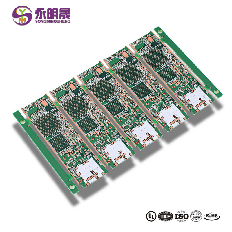
By a wide margin, most PCBs are made with 1oz copper on each layer. If your files do not include a fab print or other specifications, we'll assume 1oz finished copper weight on all copper layers. If your design requires higher voltages, resistance, or impedances, thicker copper might be necessary. There are several online tools that can help you determine what thickness, width or length your traces need to be to achieve your target results. A few such 3rd party tools are linked below. PCB Prime is not affiliated with the authors of these tools.
Copper Distribution
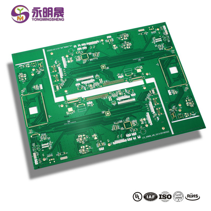
As a general rule, copper should be distributed as evenly as possible throughout your design. Not only in regard to the copper thickness on each layer, but also how it's distributed across the layer. Of course, this isn't always possible, but keep this in mind during layout.
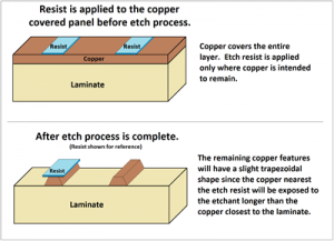
Plating and etching are organic processes in the sense that the copper clad laminate is submerged into a vat of chemicals for processing. There isn't precise control over where the copper is removed from or plated onto. During etch, the intended image is masked off to protect it from the etchant, but the chemicals in the tank dissolve the copper at slightly different rates depending on where the features are on the panel, the panel's placement within the tank itself, and how densely or sparsely the copper features are distributed.
The chemical solution in the plating and etching tanks are agitated and circulated during processing to minimize these inconsistencies; however, a panel with drastically different copper densities can prove problematic. During your design phase, try to evenly distribute your copper across the entire board rather than having large open spaces with isolated features.
HOW TO SELECT PROPER PCB COPPER THICKNESS
Selecting the optimal heavy copper thickness to apply to the plated through hole (PTH) plays a critical factor towards the overall reliability of the printed circuit board. There are two key elements to consider when determining optimal PCB copper thickness. The first is the current capacity of the barrel for acceptable heat rise. The second is the mechanical strength determined by the copper thickness, hole-size and whether or not there are any support vias.
Most customers want to build PCBs with excellent performance at an economical cost. The first step is selecting suitable copper thicknessfor your PCB type. The unique characteristics of these thickness are significant in determining the functions, performance of the PCBs. If you would like more information about PCB copper thickness selection or how to choose the best suit your PCB design, please contact us. We provide not just good advise but a complete solution. You will get smaller and smarter PCBs with excellent performance and high reliability from YMS.
Learn more about YMS products
Post time: Mar-23-2022