
Chinese PCB manufacturer tells you
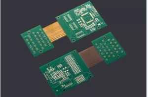
Rigid-Flex PCBs are not very new, as they were first used in a spacecraft; however, they become common when they were being used in common electronic products, especially mobile phones and laptops. Nowadays, Rigid-Flex PCBs are not only common, but they are the need. Many compact devices and appliances require Rigid-Flex PCBs.
Part 1. Key Step in Rigid Flex PCB Manufacturing
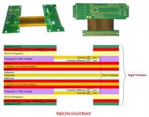
The key step of rigid-flex PCB manufacturing is removing the redundant rigid materials from the flexible layers.
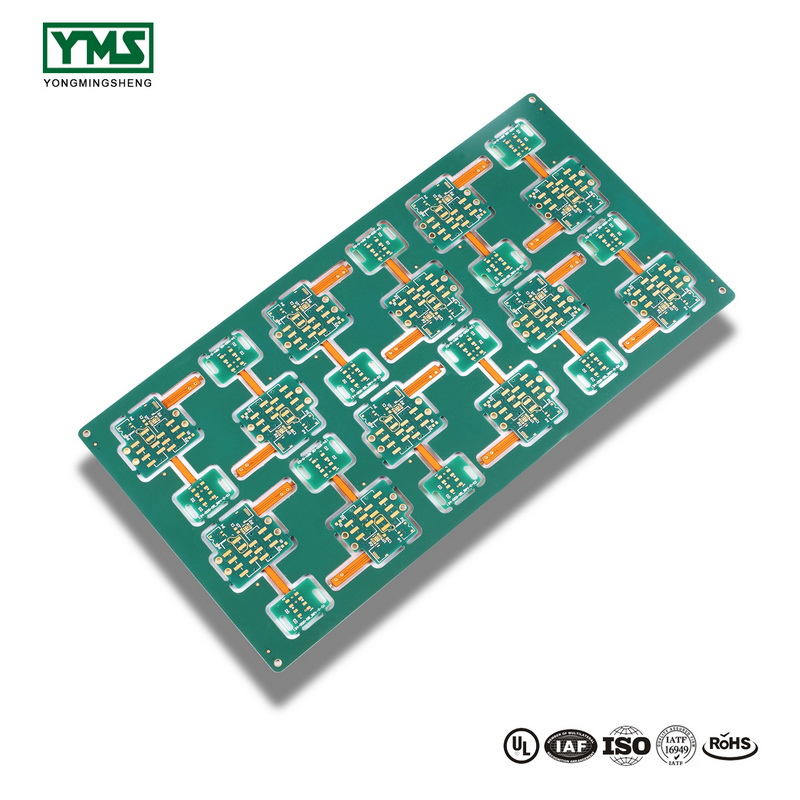
For example, the above rigid-flex PCB is manufactured by laminating 4 external rigid circuit layers on 2 flexible layers then cutting excessive rigid prepreg attached to the desired flex section by laser.
In this way, the flex section (layer 3 to 4) is exposed. We get a rigid-flex PCB that is composed of an 6-layer rigid section and a 2-layer flex section.
Knowing this, you will find it easier to understand the rigid-flex PCB manufacturing process below.
Part 2. Step-by-Step Rigid Flex PCB Manufacturing Process
Step 1. Rigid-flex PCB material preparation
Before rigid-flex PCB manufacturing, we need to pre-clean the copper-clad laminates (CCL) and cut the chemically-cleaned CCl, polyimide (PI), prepreg, coverlay, stiffeners into the desired sizes.
Step 2. Generating the inner core for flex section
Rigid-flex PCB manufacturing starts from the internal flex board, and flex board manufacturing starts from generating the flex inner core. And PI is the base material of the flex core.
If the rigid flex design has one flex layer, we laminate a thin copper foil on the PI.
If the rigid flex design has two or more flex layers, we laminate two external copper foils on PI.
Step 3. Generating circuits on flex inner core
The purpose of this step is to leave copper lines in the circuit pattern on the copper foil and remove other copper.
First, the copper foil is coated with a photoresist that can cure when UV light irradiates on it.
Then, we place a nontransparent film that draws the transparent PCB circuits on the copper foil.
Then we turn on the UV light. In this way, copper in the PCB circuit pattern is covered and protected by the cured dry film.
Next, we wash away the photoresist that is not cured with the chemical solution.
In the next, we use NaOH to solve the copper that is exposed. In this way, only the copper circuit traces are left on the inner core.
Step 4. Laminating, circuits generation, and drilling on Flex Section
Here are two cases:
If the rigid flex design has more than two flexible layers, we laminate alternating layers of PI and copper foil on the flex inner core. Then we start to generate circuits.
If the rigid flex design has one or two flexible layers, we directly go to the next process.
Circuit generation on external flex layers: this is similar to the last step, but the difference is that we remove copper in the PCB circuit pattern and keep other copper.
Then the circuit area is electroplated first with copper and then with tin.
Then we peel off the photoresist and use NaOH to etch away the copper in the non-circuit area, while the circuit area is protected by tin.
Next, tin is also removed. And now, only the electroplated copper circuit traces are kept on external flex layers.
aser drilling: We drill plated-through holes on the flex layers by laser.
Finally, we laminate coverlay on the flex layers.
Now, the flex region has been completed.
Step 5. Laminating, circuits generation, and drilling on rigid layers
Here are two cases: plated-through holes and HDI.
Rigid-flex PCB with plated-through holes: we laminate alternating layers of prepreg and copper foil on the flex region. And complete circuit generation and drilling as Step 4. The only difference is that it is mechanical drilling.
Rigid-flex PCB with HDI requirements: we laser-drill mircovias on the alternating layer of prepreg and copper foil.
And we laminate the alternating layers on the flex section.
Then we generate circuits on the rigid layers as Step 3.
Step 6. Laser-cut off the redundant prepreg outside the flex region
Here we use the laser to cut off the non-circuit prepreg area in the rigid layers so that the desired flex section is exposed.
At YMSPCB, the laser cut is smart and accurate. It won’t hurt the coverlay of the flex section.
Step 7. Complete rigid flex PCB manufacturing and testing
In this step, first, we apply the solder mask, surface finish, and silkscreen on the rigid-flex PCB surface.
Then we treat the edge of the panel, such as V-cut, half holes, etc.
Finally, we test the rigid flex PCB. The main tests are flying probe, nail-in-bed. If rigid-flex PCBs are used in automotive, medical, defense, aerospace industries, they should also pass the four-terminal sensing test.
The above is the complete rigid-flex PCB manufacturing process. If you have any concerns about rigid flex PCB manufacturing, please feel free to let us know. You can contact us from the online window on the right of the screen or by email at Joyce@ymspcb.com or kell@ymspcb.com.
You May Like
Post time: Jun-02-2022