
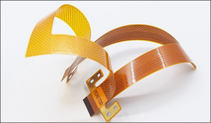
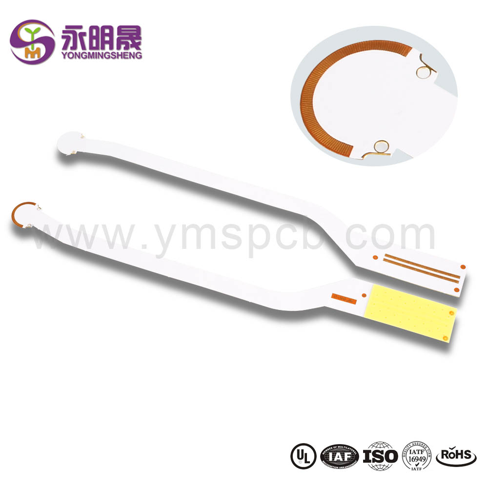
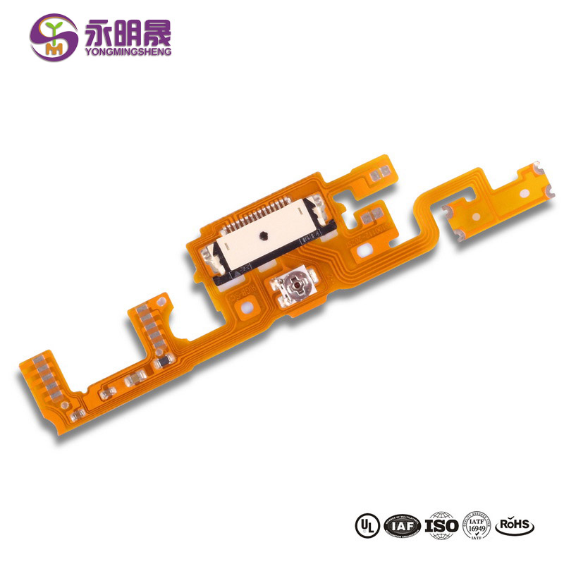
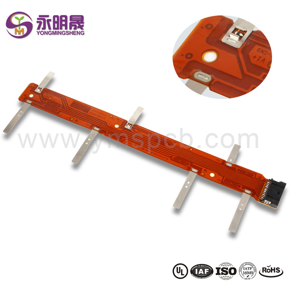
Flexible PCBs (FPC) are the PCBs that can be bent or twisted without damaging the circuits, which means the boards can be bent freely to conform to the desired shape during applications. The material the substrate used is flexible, such as Polyamide, PEEK, or a conductive polyester film.
Manufacturing process of FPC
Generally, FPC are made through a photolithographic technology sheet by sheet. Recently, a more advanced way to produce FPC is RTR (roll to roll) lamination.
First let’s learn about photolithographic technology:
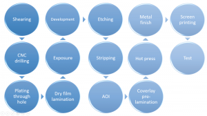
Flow chart of the FPC manufacturing process
Photolithographic technology
1. Shearing:
To optimize the material utilization, cut the material as working size for different design and layout concern.
2. CNC (computer numerical control) drilling:
To fit customers’ design and process demand, drill different holes on boards, such as alignment holes, testing vias, components holes, etc.
3. Plating through hole:
Since both the top and bottom layer are not conductive, plate copper on the hole-wall after drilling to realize pattern connection between layers. This process applies to the making of double-sided flexible boards.
4. Dry film lamination:
To create an etching resist layer, pass pre-treated boards through hot roller to laminate dry film on it.
5. Exposure:
Transfer the designed circuit pattern image to dry film laminated on the foil to create an exposure area.
6. Development:
Cast UV (ultraviolet) light on the dry film, the dry film on the exposure area will be polymerized and hardened, and the dry film on non-exposure area can be removed and expose copper.
7. Etching:
After development, non-exposure area will be moved away by chemical reaction and the protected area will be remained.
8. Stripping:
After etching, remove the dry film covering the circuit pattern and make pattern exposed.
9. AOI (automated optical inspection):
Use AOI tester to check the quality of circuit.
10. Coverlay pre-lamination:
The board will be covered with insulating layer called ‘coverlay’ to protect the circuit.
11. Hot press:
The board with coverlay pass through hot press machine to form adhesion between copper and coverlay.
12. Metal finish:
Coat the bonding area with nickel or gold to protect and keep the terminator’s function.
13. Screen printing:
If there’re needs to print visible information like logos or numbers onto the boards, silk screening will be applied.
14. Test:
Carry out electrical and functional test to detect the defects of finished circuits.
More than 10 years' efforts in this industry, YMSPCB has been focusing on advanced PCB fabrication including Flex PCBs, Flex-Rigid PCBs, HDI PCBs, MCPCBs etc. with mixed volume from prototype, low-to-mid volume to high volume production in order to meet your diversified needs. Contact Us now with your specific needs and we'll allow optimal products within your reach.
Learn more about YMS products
Post time: Jun-02-2022