
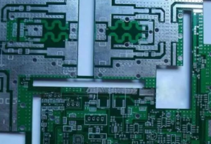
What is High-Frequency PCB
High-frequency PCBs generally provide a frequency range of 500MHz to 2 GHz, which can meet the needs of high-speed PCB design, microwave, radiofrequency and mobile applications. When the frequency is higher than 1 GHz, we can define it as high frequency.
Today, the complexity of electronic components and switches keeps increasing, and a faster signal flow is required than usual. Therefore, a higher transmission frequency is required. When integrating special signal requirements into electronic components and products, high-frequency PCB has many advantages, such as high efficiency, fast speed, low attenuation, and constant dielectric constant.
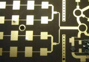
High-frequency PCB - special materials
Special materials are needed to realize the high frequency provided by this type of printed circuit board, Because any change of their permittivity may affect the impedance of the PCBs. Many PCB designers choose Rogers dielectric material because it has lower dielectric loss, lower signal loss, lower circuit manufacturing costs, and is more suitable for rapid turnaround prototype applications among other materials.
High Frequency PCB Layout Skills
1. The less the lead between the high-speed electronic device pins bent the better
The lead wire of the high-frequency circuit wiring is preferably a full line, which needs to be turned, and can be folded by a 45-degree line or a circular arc. This requirement is only used to improve the fixing strength of the copper foil in the low-frequency circuit, and in the high-frequency circuit, the content is satisfied. One requirement is to reduce the external transmission and mutual coupling of high frequency signals.
2. The high frequency circuit device between the pin layers alternately less as possible
The so-called "the least alternating between the layers of the leads is better" means that the fewer via used in the component connection process, the better. A via can bring about a distributed capacitance of about 0.5pF, and reducing the number of via can significantly increase speed and reduce the possibility of data errors.
3. The lead between the high-frequency circuit device pins is as short as possible
The radiant intensity of the signal is proportional to the length of the trace of the signal line. The longer the high-frequency signal lead, the easier it is to couple to the component close to it, so for clocks such as signals, crystal, DDR data, High-frequency signal lines such as LVDS lines, USB lines, and HDMI lines are required to be as short as possible.
4. Pay attention to "crosstalk" introduced by signal line and short distance parallel line
The Big Three Problems of High Speed PCB Design
When working on a high speed PCB design, there are a ton of issues that you’ll encounter along the way towards getting your signals interact from point A to point B. But of them all, the top three concerns to be aware of are:
Timing. In other words, are all of the signals on your PCB layout arriving at the proper time in relation to other signals? All of the high speed signals on your board layout are controlled by a clock, and if your timing is off, then you’ll likely be receiving corrupted data.
Integrity. In other words, do your signals look as they should when they arrive at their end destination? If they don’t, then it means that your signal likely encountered some interference along the way that ruined its integrity.
Noise. In other words, did your signals encounter any kind of interference along their journey from transmitter to receiver? Every PCB emits some kind of noise, but when too much noise is present, then you increase the chance of data corruption.
Now, the good news is that these Big Three Problems you might encounter on a high speed PCB design can all be corrected by these Big Three Solutions:
Impedance. Having the proper impedance between your transmitter and receiver will have a direct impact on the quality and integrity of your signals. This will also affect how sensitive your signals are to noise.
Matching. Matching the lengths of two coupled traces will ensure that your traces arrive at the same time and in sync with your clock rates. Matching is an essential solution to look at for DDR, SATA, PCI Express, HDMI, and USB applications.
Spacing. The closer your traces are to each other, the more susceptible they become to noise and other forms of signal interference. By not placing your traces closer than they need to be, you’ll reduce the amount of noise on your board.
If you want to know more about the price of the high-frequency PCB, please leave your message and get ready your PCB files (Gerber format preferred). We will connect with you and quote you as quickly as possible.
Learn more about YMS products
Post time: Mar-14-2022