
Multilayer PCB manufacturing from 4 to 60 Layers | YMSPCB

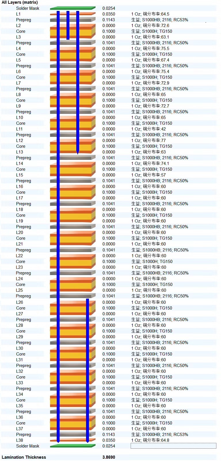
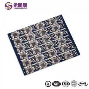
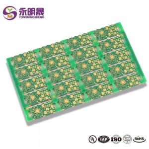
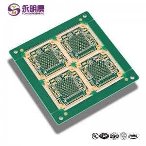
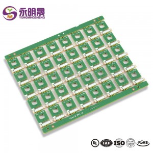
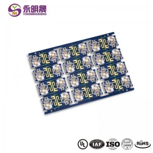
The multilayer PCB refers to a printed circuit board with more than two layers, which is composed of interconnected lines on several layers of insulating substrates and pads for assembling and soldering electronic components. It has the function of conducting each layer of lines and insulating each other. High-speed PCBs are generally designed with multilayer PCB. Common multilayer boards are generally 4-layer boards or 6-layer boards, and complex multi-layer boardscan reach dozens of layers.
YMS Multilayer PCB manufacturing capabilities:
| YMS Multilayer PCB manufacturing capabilities overview | ||
| Feature | capabilities | |
| Layer Count | 3-60L | |
| Available Multilayer PCB Technology | Through hole with Aspect Ratio 16:1 | |
| buried and blind via | ||
| Hybrid | High Frequency Material such as RO4350B and FR4 Mix etc. | |
| High Speed Material such as M7NE and FR4 Mix etc. | ||
| Thickness | 0.3mm-8mm | |
| Minimum line Width and Space | 0.05mm/0.05mm(2mil/2mil) | |
| BGA PITCH | 0.35mm | |
| Min mechanical Drilled Size | 0.15mm(6mil) | |
| Aspect Ratio for through hole | 16:1 | |
| Surface Finish | HASL, Lead free HASL,ENIG,Immersion Tin, OSP, Immersion Silver, Gold Finger, Electroplating Hard Gold, Selective OSP,ENEPIG.etc. | |
| Via Fill Option | The via is plated and filled with either conductive or non-conductive epoxy then capped and plated over(VIPPO) | |
| Copper filled, silver filled | ||
| Registration | ±4mil | |
| Solder Mask | Green, Red, Yellow, Blue, White, Black, Purple, Matte Black, Matte green.etc. | |
Learn more about YMS products
Read more news

The Features of Multilayer PCB
The biggest difference between a multilayer PCB and a single-sided or double-sided PCB is the addition of an internal power layer and a ground layer. The power line and ground network are mainly arranged on the inner electrical layer.
However, the circuit layout of multilayer PCB is mainly based on the top and bottom layers, supplemented by the middle circuit layer. Therefore, the design of a multi-layer PCB is basically the same as that of a double-sided PCB.
The key is how to optimize the circuit layout of the inner electrical layer so that the circuit layout of the circuit board is more reasonable and the electromagnetic compatibility is better.
From a technical point of view, multilayer PCBs present several advantages in design. These benefits multilayer PCBs present include:
• Small Size: One of the most prominent and lauded benefits of using multilayer PCBs lies in their size. Because of their layered design, multilayer PCBs are inherently smaller than other PCBs with similar functionality. This presents a major benefit to modern electronics, as the current trend is working toward smaller, more compact yet more powerful gadgets like smartphones, laptops, tablets and wearables.
• Lightweight Construction: With smaller PCBs comes less weight, especially as the multiple connectors required to interlink separate single and double-layered PCBs are eliminated in favor of a multilayered design. This, again, is beneficial for modern electronics, which are geared more toward mobility.
• High-Quality: Due to the amount of work and planning that must go into the creation of multilayer PCBs, these types of PCBs tend to be better in quality than single and double-layer PCBs. They also tend to be more reliable as a result.
• Increased Durability: Multilayer PCBs tend to be durable by their nature. Not only do these multilayer PCBs have to withstand their own weight, but they must also be able to handle the heat and pressure used to bind them together. On top of these factors, multilayer PCBs use multiple layers of insulation between circuit layers, binding it all together with prepreg bonding agent and protective materials.
• Enhanced Flexibility: Though this does not apply to all multilayer PCB assemblies, some do use flexible construction techniques, resulting in a flexible multilayer PCB. This can be a highly desirable trait for applications where mild bending and flexing may occur on a semi-regular basis. Again, this does not apply to all multilayer PCBs, and the more layers incorporated into a flexible PCB, the less flexible the PCB becomes.
• More Powerful: Multilayer PCBs are extremely high-density assemblies, incorporating multiple layers into a single PCB. These close-quarters enable boards to be more connective, and their innate electrical properties allow them to achieve greater capacity and speed despite their smaller size.
• Single Connection Point: Multilayer PCBs are designed to work as a singular unit, rather than in tandem with other PCB components. As a result, they have a single connection point, rather than the multiple connection points required to use multiple single layer PCBs. This proves to be a benefit in electronic product design as well since they only need to include a single connection point in the final product. This is particularly beneficial for small electronics and gadgets designed to minimize size and weight.
These benefits make multilayer PCBs highly useful in a variety of applications, particularly mobile devices and high-functioning electronics. In turn, with so many industries turning to mobile solutions, multilayer PCBs are finding a place in an increasing number of industry-specific applications.
What is Multilayer PCB?
PCB can be divided into single-sided, double-sided, and multi-layered boards from the structure.
The multilayer PCB refers to a printed circuit board with more than two layers, which is composed of interconnected lines on several layers of insulating substrates and pads for assembling and soldering electronic components. It has the function of conducting each layer of lines and insulating each other. High-speed PCBs are generally designed with multilayer PCB. Common multilayer boards are generally 4-layer boards or 6-layer boards, and complex multi-layer boards can reach dozens of layers.
Products categories
-

Wholesale Multi Layer PCB-PCB Manufacturer Chin...
-
Wholesale Castellated Multilayer PCB from China...
-
Edge Plating PCB 10 Layer Board edge plating PC...
-
HDI Multilayer PCB-China PCB Manufacturer | YMSPCB
-

LED display screen pcb HDI laser via in PAD cop...
-
FR4 Multilayer PCB-Chian Wholesale Supplier | Y...


