
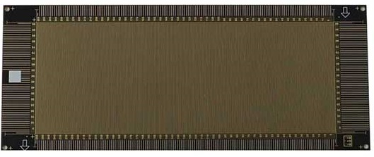
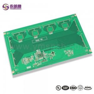
SMD LED display screen pcb Micro led pcb mini led BT| YMSPCB

Waht is SMD LED BT Substrate:
SMD LED BT Substrate refers to THE PCB that is manufactured with BT Materials and applied to SMD LED products.Different from normal PCB, BT Materials is applied in MD LED BT Substrate, which is mainly product by Mistubishi Gas Chemical Co., Inc.The BT Materials made of B (Bismaleimide) and T (Triazine) resin has the advantages of high TG (255~330°C), heat resistance (160~230°C), moisture resistance, low dielectric constant (DK) and low dissipation factor (Df). SMD LED is a new surface mount semiconductor light-emitting device , with a small scattering angle is large , light uniformity, high reliability , light colors including white colors , it is widely used in a variety of electronic products . PCB board is one of the major manufacturing SMD LED material .
Difference between SMD and COB LED
SMD refers to the term “Surface Mounted Device” LEDs, which are the utmost shared LEDs in the market. The LED chip is eternally fused to a printed circuit board (PCB), and it is especially popular because of its versatility. he PCB is built on a rectangular-shaped, flat object, which is what we usually see as SMD. If you look into SMD LED closely, you can see a small black point right in the center of the SMD; that is the LED chip. You can find it in light bulbs and filament lights and even in the notification light on your mobile phone.
One of the latest developments in LED industry is COB or “Chip on Board” technology which is a step forward for more efficient energy use. Similar to SMD, COB chips too have multiple diodes on the same surface. But the difference among LED light COB and SMD is that COB LEDs have more diodes.
Advantages of SMD LED
1) The SMD is more flexible, and the display of its chips is decided according to the printed circuit board layout, and it can be altered to meet different engineering solutions.
2) SMD light source has a bigger illumination angle of up to 120 & Phi; 160 degrees, small size and light weight of electronic products, high assembly density and the size and weight of the cover components are only about 1/10 of that of conventional plug-in components.
3) It has high reliability and strong anti-vibration capability.
4) Low solder joint defect rate and improve production efficiency.
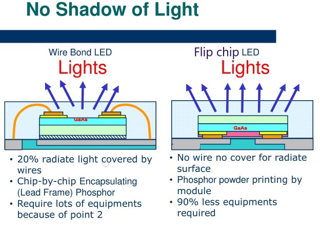
Schematic diagrams of wire bonding and flip chip
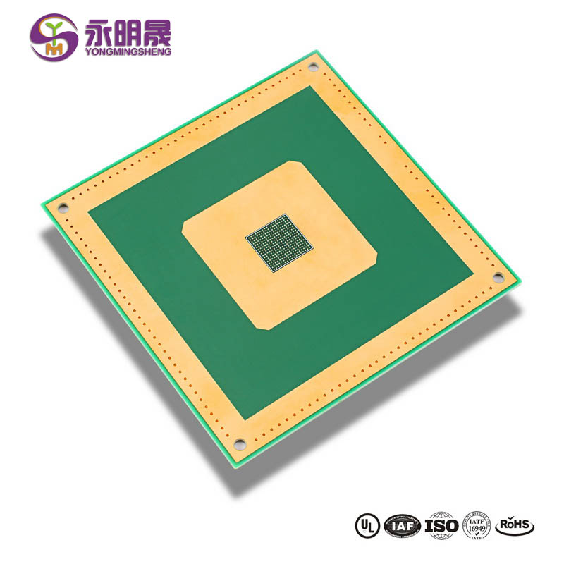
YMS SMD LED display screen pcb manufacturing capabilities:
| YMS SMD LED display screen pcb manufacturing capabilities overview | |
| Feature | capabilities |
| Layer Count | 1-60L |
| Available SMD LED display screen pcb Technology | 1+N+1 |
| 2+N+2 | |
| 3+N+3 | |
| 4+N+4 | |
| 5+N+5 | |
| Any layer | |
| Thickness | 0.3mm-6mm |
| Minimum line Width and Space | 0.05mm/0.05mm(2mil/2mil) |
| Light Emitting Diode PITCH | P0.47mm;P0.58mm;P0.70mm;P0.77mm;P0.925mm;P1.0mm;etc. |
| Min laser Drilled Size | 0.075mm(3nil) |
| Min mechanical Drilled Size | 0.15mm(6mil) |
| Aspect Ratio for laser hole | 0.9:1 |
| Aspect Ratio for through hole | 16:1 |
| Surface Finish | HASL, Lead free HASL,ENIG,Immersion Tin, OSP, Immersion Silver, Gold Finger, Electroplating Hard Gold, Selective OSP,ENEPIG.etc. |
| Via Fill Option | The via is plated and filled with either conductive or non-conductive epoxy then capped and plated over |
| Copper filled, silver filled | |
| Laser via copper plated shut | |
| Registration | ±4mil |
| Solder Mask | Green, Red, Yellow, Blue, White, Black, Purple, Matte Black, Matte green.etc. |
Learn more about YMS products
Read more news


Products categories
-

HDI printed circuit boards 8Layer 2 Step HDI Bo...
-

Micro via PCB HDI PCB 8L 1+N+1 Via on PAD| YMSPCB
-

LED display screen pcb HDI laser via in PAD cop...
-

HDI pcb any layer hdi pcb high speed insertion ...
-

Any layer hdi pcb 12Layer Staggered Vias Immers...
-

HDI PCB 2+n+2 VIPPO High Density Interconnect P...


