
It is now popular that the HDI PCB has better and advanced features than what we have been seeing on the traditional PCBs. Since that is the case, it implies that the circuit board has some advantages that it has over the former.
Here are some of the features, properties, and advantages of the HDI PCB:
1. Less Heat Transfer
It is no secret that the presence and dominance of heat on a Printed Circuit Board (PCB) can be the singular reason why it may damage in a short while.
Something can be done about that. It is by reducing the presence of heat and transferring the same in time.
The HDI PCB does that excellently. The circuit board does a great job of facilitating the transfer of less heat. At the same time, the heat will be made to travel farther before its escape from the High Density Interconnector (HDI) circuit board.
2. Extended Battery Life
You must care for the batter life and longevity of the HDI PCB, as much as you are caring for the performance.
It must be mentioned that the High Density Interconnector has a higher and extended battery life because of the reduced power consumption.
3. Reliable Transmission
The reliability of transmission on the HDI PCB is because of the compact size that comes in handy when adding more components.
That is the reason why the addition and incorporation of the BGA and OFP packages wouldn’t be a tough task because the HDI circuit board can accommodate them because of their smaller sizes, and because of the more space on the circuit board.
4. Populated Sides
The sides of the HDI circuit board are populated. The reason is that it allows the PCB designer and manufacturer more space to add more components that will make the job successful.
5. Reducing the Weight of Products
The use of the HDI circuit board plays an excellent role in the reduction of the weights of products.
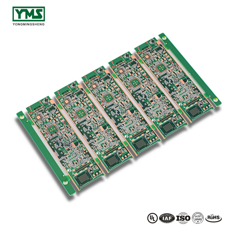
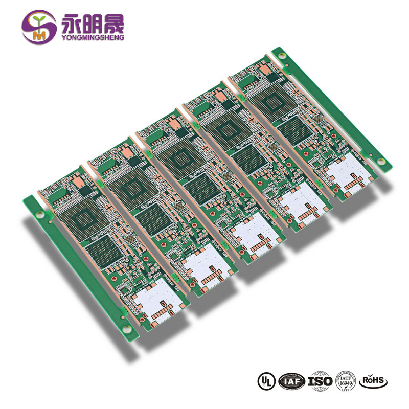
You will recall that the board has a compact size that makes it easier for it to fit into any type of product to be designed and manufactured. Also, it hides the wires very well so that wouldn’t be an obstruction during the coupling. HDI PCBs have been used widely to reduce the entire size and weight of final products while enhancing the electrical performance. For these medical devices like pacemakers, miniaturized cameras, and implants, only HDI techniques are capable of supplying small packages with fast transmission rates. HDI PCBs are responsible for smaller portable products, such as smartphones, tablets, and wearable electronics. Automotive devices, military, and aerospace equipment also need the support of HDI technologies.YMS as a professional PCB manufacturer can provide high-quality HDI PCB for customers from home and abroad.
You May Like
Post time: Dec-08-2021