
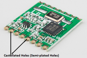
Castellated Holes or Castellations are indentations created in the form of semi-plated holes on the edges of the PCB boards. These Castellations help to mount one PCB board on top of another during assembly. Depending upon the application, instead of half holes, they may also look like a small or larger portion of a broken circle. Such holes are designed to provide proper alignment between the boards while soldering. This mounting process takes place with the help of castellated holes and called board-to-board soldering. Castellated holes are created on various PCB modules (Bluetooth or Wi-Fi modules), these modules can then be used as independent parts to be mounted onto another board during the assembly process.
Through Hole Technology (THT) and Surface Mount Technology are commonly used during PCB assembly process. Apart from these, board-to-board soldering is used, when there is a need to mount a board on the top of another PCB. Castellations serve as a link between the module and the board onto which the module has to be soldered.
Why do we use Castellated holes?
By creating these holes on the board edges, they can be used to replicate certain parts of a PCB circuit. For example, if there is a circuit that includes an inverter, filter, or feedback loops. These small sub-circuits can be mass-produced, tested and can be soldered on to the main PCB that contains other parts of the circuit whenever required.
Use of Castellated Holes:
- Castellated PCBs can be used as breakout boards for a particular portion of the larger PCB.
- These holes give ease to change the Pin layout of the component as per the user requirement.
- Integrated modules can be produced on a single PCB board using castellation, which can be used further into another assembly during production.
- PCBs with castellated holes can be mounted easily to another PCB during final production.
- They are used to combine two boards to validate the solder joint quality.
- They are used for breakout boards or small modules like Wi-Fi modules.
- Castellated holes also help to create wireless PCB to PCB links.
PCB Manufacturing Process for Electroplating Half Holes
The manufacture of a conventional castellation hole is a simple step. Designers begin with drilling, followed by the application of chemical copper, and then panel plating. Later on, image transfer follows, followed by pattern plating, and then stripping the film. Etching, solder mask printing, and surface finishing soon follow. The final process is hole castellation and outline milling.
However, the above steps lead to a decrease in the performance and yield of the entire product. Today, the formation of castellated holes is somewhat different. While it doesn’t drift far away from the traditional method, it’s slightly different.
The formation of castellated holes begins with drilling the substrate plate edge. Here, specialized drilling equipment is a necessity. Without special drilling equipment, everything else that follows might go wrong. After preparing, plating through the hole then follows. Plating is of high importance; the scale ensures a copper layer on the hole wall. The copper layer brings about the excellent conductivity of a board’s components.
Panel plating is the third step
Panel plating gives room for even copper distribution on the panel. After the completion of panel plating, image transfer follows. Image transfer is the transfer of the conductor pattern. The transfer of the way is from the film master to the copper-clad base material. After that, pattern plating follows. Pattern plating is masking off a majority of copper surfaces. It’s all about plating only the pads and traces of the circuit pattern.
Striping is the sixth step of PCB manufacturing for electroplating half holes. Etching soon follows stripping. Etching of the substrate to eliminate exposed copper is the seventh step; the solder-mask application comes after the etching process. The application of a solder-mask is to shield the PCB from oxidation.
Surface coating follows solder masking. The surface coating shields the exposed copper circuitry. It also provides a solderable surface during the assembly of PCBA components. Plating half a hole in the last step. Plating the half holes allows for the desired electrical flow through the entire board.
Summary
Castellated holes are essential. They find heavy use in computer applications, automobiles, industrial control, and telecommunications. Do you have any castellated holes projects? Do you want to learn how to use castellated hole technology better in PCB production?
We understand the stacking conditions and the manufacturing process of half holes. Our products meet ISO9001, RoHS, and UL standards. Are you in need of a high-quality castellated hole in your design? Let us assist you. With us, you’ll find nothing but the best-castellated holes in your system. At a suitable time, feel free to contact us to discuss more in regards to PCB technology.
Post time: Aug-20-2022