
2 Layer PCB Manufacturer in China
The 2 layer PCB ( double-sided PCB )is a printed circuit board with copper coated on both sides, top and bottom. There is an insulating layer in the middle, which is a commonly used printed circuit board. Both sides can be layout and soldered, which greatly reduces the difficulty of layout, so it is widely used.
To use circuits on both sides, there must be a proper circuit connection between the two sides, as shown in the pictures right. The “bridges” between such circuits are called vias. A via is a small hole on the PCB board filled or coated with metal, which can be connected with the circuits on both sides. Because the area of the double-sided board is twice as large as that of the single-sided board, the double-sided board solves the difficulty of the single-sided board due to the interlaced layout (it can be connected to the other side through the holes), and it is more suitable for more complicated circuits than the single-sided board.
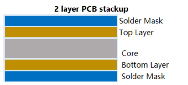
It's clear that layer 1, or the top layer is a signal layer on the 2 layers PCB stack up. Both the top layer and the bottom layer are copper layers.
Choose Your 2 Layer PCB
We put at your disposal our know-how for the most complex printed circuit designs with parameters or characteristics so special that they require the personal assistance of our team. We will provvide customized solutions that meet your needs simply by sending us your files by e-mail.
Double-Sided PCB: The Ultimate FAQ Guide
Double-sided PCBs are commonly found in many electronics used each day. While single-sided PCBs have one conductive surface, double-sided PCBs have a conductive layer on each side. A dielectric layer is surrounded by circuit copper layers and solder mask on both sides.
While single-sided PCBs have one conductive surface, double-sided PCBs have a conductive layer on each side. A dielectric layer is surrounded by circuit copper layers and solder mask on both sides. Vias allow manufacturers to create traces on both sides that route around each other and connect between layers.
The uses or applications of the double-sided PCB are described as under:
They are used in the converters of different appliancesThey are used in the regulators to control the amount of current flowing through the circuitPower conversion elements also include the double-sided PCB Instrumentation also makes the use of the double-sided PCB.
The majority of the control relays control the highest quality of two-layered PCB Power supplies are also the best applications of this PCB UPS systems and their batteries contain the premium quality of two-layered PCB The voltage regulators have the best two-layered PCB.
The motherboard of the Personal Computer is also made up of premium-level PCB This board is also used in the line reactors circuitry You'll also fnd the double-sided PCB in the traffc control systems Many lightning devices are also known to operate with this type of PCB.
A. More flexibility for designers.
B. Increased circuit density.
C. Relatively lower costs.
D. Intermediate level of circuit complexity.
E. Reduced board size (which can reduce costs)
The difference is that instead of using a single-sided copper core, the manufacture will start a core with copper on both sides. During production, they also drill holes called vias that they can plate or fill with a conductive, or non conductive material.
Double-sided PCB design takes the same high-quality schematic design, layout, and production planning tools that you would use for a highly complex board. With these simpler boards, you can use easier routing strategies that greatly simplify your layout.
While single-sided PCBs have one conductive surface, double-sided PCBs have a conductive layer on each side. A dielectric layer is surrounded by circuit copper layers and solder mask on both sides. Vias allow manufacturers to create traces on both sides that route around each other and connect between layers.
YMS PCB Besides the availability of PCB at reasonable rates, some other factors that are responsible for makingChina the best place for two-layered PCB production are:
1、Use of all modern technologies in the production of high-quality PCBInspection by the experienced individuals.
2、Fulfillment of all quality and safety standards while making the PCB.
The warranty period of the double-sided PCB ranges from three to five straight years.
Contact the most efficient manufacturer in China.
Contact their support team for getting an idea of the items present.
Choose your best pick about the double-layered circuits.
Check the availability of all those documents that are required for the import of the PCB.
Cutting —> Drilling —> Sinking/1ST Copper Plating —> Layout —> Pattern Plating/2nd Copper Plating —> Etching —> Solder Mask —> Legend Printing —>Immersion Tin (or Immersion Gold) —> CNC Routing —> V Cut (some boards do not need this) —> Flying Probe Test —> Vacuum Packaging
The typical PCB thickness is 0.063inches or 1.57mm; it is a standardized level defined from the past. That isbecause, during the plywood industry 0.063" was the thickness of the plywood sheets used as substrates foielectronic devices. which included PCBs.
1. Ensure Tight Component Placement
2. Have A Section That Separate Digital and Analog Circuitry
3. Maintain Short Signals
4. Employ Analog Ground
5. Maintain Clear Return Paths Of the Analog Signal
There is no doubt that 4 layers PCB is more expensive than 2 layers PCB because of complexity of design and higher sensitivity. What’s more, there is a factor 4 layers PCB cost what the higher quality of signals, achieving by decreasing distortion and propagation levels. So more and more electronic engineers prefer to 4 layers PCBs due to the higher levels of signal integrity and reduced interference levels.
Single-sided PCB traces are present on only one side, while double-sided PCBs have traces on both sides with top and bottom layers. The components and conductive copper are mounted on both sides of a double-sided PCB, and this leads to the intersection or overlap of the trace
If you cannot find an answer to your question in our FAQ, you can always contact us and we will be with you shortly.