
PCBs are the basis of all electronic devices, without which that device cannot function. Essentially PCBs, also known as Printed Circuit Boards, consist of electric components and conductive traces that are built onto a board to help connect the components and to direct electricity. PCBs can be divided into distinctive types; one of them is Multilayer PCBs.
What are Multilayer PCBs?
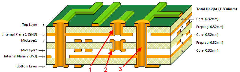
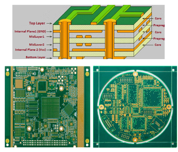
Multilayer PCBs, as the name suggest are a combination of different layers. Single sided PCBs and double sided PCBs are both combined to give this complex designed PCB. Multilayer PCBs have increased number of layers and therefore have increased area available for wiring. The boards are made by combining double layered PCBs and separating them with insulating material such as dielectric.
How to Design Multilayer PCB
Designing a single or double layer PCB is easy and can be done by any hobbyist with a few components, which are easily available in the market. A DIY article to design a single layer PCB will be available soon.
As a professional PCB designer, I have some tips for you, that will help you in designing the multi-layer PCB efficiently.
- Always try to add an even number of PCB layers. Since both layers carry signals, the difference in the price segment for odd layers isn’t much. You will also rarely find a manufacturer who produces odd layers at much lower prices.
- Choose the right PCB thickness, keeping in mind the number of heavy components on the PCB board.
For example, you can consider PCB with 0.8 thickness if all of the components are lightweight. The thickness support in multilayer PCB design varies with different vendors. However, some standard PCB thickness sizes are 0.8mm, 1mm, 1.2mm, 1.6mm. - Select the PCB stack, as per the design requirements. The PCB engineer selects the method of ground and power planes totally based on the circuit design.
- Communicate effectively with the manufacturer and understand the capabilities of the PCB manufacturing.
- Cross-check Schematic connections with PCB design and footprints with schematic symbols.
- Once the design process is finished, the PCB is ready to get manufactured. This takes me back to the time, when I designed my first multi layer PCB(4 layers) and sent it to a local manufacturing house. I waited for it like a school going kid awaiting his results.I was keen on knowing how the design will turn out to be!
- So, yes, Manufacturing stage of PCB is a crucial part of the whole process. It is the time when your design gets a physical form.
- In order to send your PCB to the manufacturer, you will need to get the gerber file of the PCB. A gerber file is the standard output file for a multilayer PCB, inbuilt in any of the softwares you choose for your design.
- Check if there is an issue with minimum trace width or minimum copper clearance or that the minimum hole size criteria matches or not. If you detect any such issue, you might have to edit it to reproduce the PCB.
- The manufacturing process consists of laminating inner different copper layers with prepreg and the dielectric material. The lamination process is done under high temperature and is very critical as the PCB holes need to be matched. A minor difference of layer placement in manufacturing causes noise or even short circuit in PCB, therefore, this process needs to be done with high accuracy. It also takes care of trapping any air bubble so the PCB layers are tightly glued together with epoxy chemicals (industrial glue). The popular materials used for the lamination process are basic epoxy glass, exotic ceramic, and Teflon materials.
Multi-Layer PCB manufacturing process
- Once the design process is finished, the PCB is ready to get manufactured. This takes me back to the time, when I designed my first multi layer PCB(4 layers) and sent it to a local manufacturing house. I waited for it like a school going kid awaiting his results.I was keen on knowing how the design will turn out to be!
- So, yes, Manufacturing stage of PCB is a crucial part of the whole process. It is the time when your design gets a physical form.
- In order to send your PCB to the manufacturer, you will need to get the gerber file of the PCB. A gerber file is the standard output file for a multilayer PCB, inbuilt in any of the softwares you choose for your design.
- Check if there is an issue with minimum trace width or minimum copper clearance or that the minimum hole size criteria matches or not. If you detect any such issue, you might have to edit it to reproduce the PCB.
- The manufacturing process consists of laminating inner different copper layers with prepreg and the dielectric material. The lamination process is done under high temperature and is very critical as the PCB holes need to be matched. A minor difference of layer placement in manufacturing causes noise or even short circuit in PCB, therefore, this process needs to be done with high accuracy. It also takes care of trapping any air bubble so the PCB layers are tightly glued together with epoxy chemicals (industrial glue). The popular materials used for the lamination process are basic epoxy glass, exotic ceramic, and Teflon materials.
Summary
YMS is one of the top manufacturers of multilayer PCBs. They have a global supply chain and they deliver all over the world. You can upload the designs online using their web app, and you need to place the final order only after getting the right quote.
Post time: Aug-17-2022