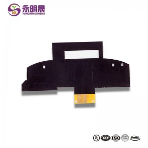
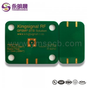
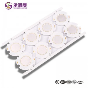
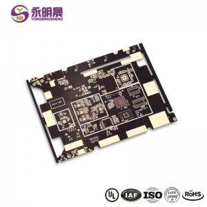
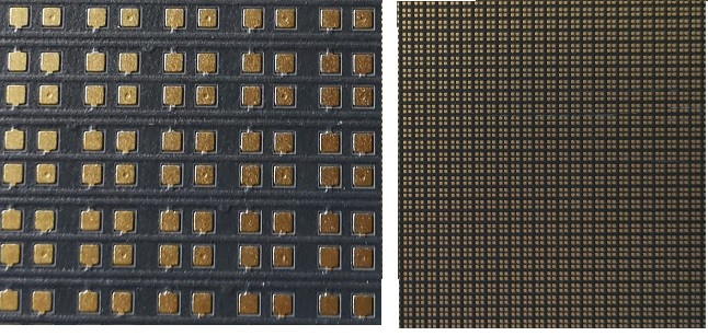
LED 디스플레이 화면 PCB HDI 레이저 비아 인 PAD 구리 도금 종료 | YMSPCB

발광 다이오드 표시 스크린 인쇄 회로 기판:
LED 스크린, LED 비디오 월, LED 패널 또는 LED 사이 니지로도 알려진 LED 디스플레이는 점진적으로 기존 광고판, 라이트 박스 등을 고유 한 장점으로 대체했습니다. LED 디스플레이 광고는 미디어 산업의 새로운 힘이되었습니다.
기존 광고는 이미지 만 표시 할 수 있지만 LED 디스플레이 / LED 디스플레이 / LED 화면은 텍스트, 그림, 비디오 및 사운드의 완벽한 조합이 될 수 있으며 필요에 따라 프레젠테이션을 변경할 수 있습니다.
디스플레이 플레이어 소프트웨어 설정을 통해 유연하게 재생할 수 있으며 고해상도, 고휘도 및 풀 컬러를 제공합니다!
LED 디스플레이 광고 화면은 보행자의 관심을 쉽게 끌 수 있으며 기억하기 쉬워 더 큰 광고 효과를 낼 수 있습니다.
LED 디스플레이는 이제 미디어 광고, 교통, 보안, 부동산 및 무대 공연 배경에서 널리 사용됩니다.
LED 디스플레이는 아름답고 쉽게 손상되지 않으며 수명이 길어 불필요한 비용과 비용을 많이 절약 할 수 있습니다.
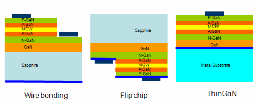
Schematic diagrams of wire bonding flip chip and ThinGaN LEDs
YMS LED 디스플레이 화면 PCB 제조 능력 :
| YMS LED 디스플레이 화면 PCB 제조 기능 개요 | |
| 특색 | 능력 |
| 레이어 수 | 1-60L |
| 사용 가능한 LED 디스플레이 화면 PCB 기술 | 1 + N + 1 |
| 2 + N + 2 | |
| 3 + N + 3 | |
| 4 + N + 4 | |
| 5 + N + 5 | |
| 모든 레이어 | |
| 두께 | 0.3mm-6mm |
| 최소 라인 너비 및 공간 | 0.05mm / 0.05mm (2mil / 2mil) |
| 발광 다이오드 PITCH | P0.47mm, P0.58mm, P0.70mm, P0.77mm, P0.925mm, P1.0mm 등 |
| 최소 레이저 드릴 크기 | 0.075mm (3 무) |
| 최소 기계 드릴 크기 | 0.15mm (6mil) |
| 레이저 홀의 종횡비 | 0.9 : 1 |
| 관통 구멍의 종횡비 | 16 : 1 |
| 표면 마감 | HASL, 무연 HASL, ENIG, 침지 주석, OSP, 침수은, 금 핑거, 전기 도금 하드 금, 선택적 OSP, ENEPIG.etc. |
| 채우기 옵션을 통해 | 비아는 전도성 또는 비전 도성 에폭시로 도금되고 채워진 다음 캡핑되고 위에 도금됩니다. |
| 구리 충전,은 충전 | |
| 구리 도금 차단을 통한 레이저 | |
| 기재 | ± 4mil |
| 솔더 마스크 | 녹색, 빨간색, 노란색, 파란색, 흰색, 검은 색, 보라색, 무광택 검정색, 무광택 녹색 등. |
- It is beneficial to use LED PCB as it helps electronics get thinner and smaller. Its numerous applications include but not limited to:
-
1. Telecom LED PCB
Telecommunication devices use LED displays and indicators. The LEDs offer decreased weight, improved durability, and enhanced heat transfer. So, they are much useful in the telecom sector applications such as high-frequency amplifiers and filtering appliances.
-
2. Automotive LED PCB
They can be found in car indicators, brake lights, headlights, and other devices. Longevity, durability, and low prices are the reason that LED PCBs aluminum PCB are common in the automotive industry.
-
3. Computer LED PCB
They are also becoming common in computer equipment as indicators and displays. The LED PCB board is an ideal solution for the heat-sensitive computer machinery.
-
4. Medical LED PCB
In medical examinations and surgeries, high-powered LED lighting tools are used. They ensure the proper function of the medical equipment regardless of the number of patients in the medical office.
-
5. Other LED PCB
Other application fields of LED PCB board are airport runway lights, street lighting, photovoltaic (solar) lightening, lanterns and flashlights, highway tunnel lightening, highway growth plant, signal, and traffic lighting.
LED PCBs are best for consumer devices, some marine and aviation applications, flashlight and other camping accessories in lower-light environments, elevator lighting, power converters, decorative and concealed lights, and many more