
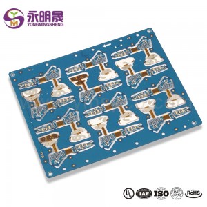
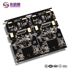
China PCB 6Layer Gold Finger Blue Soldermask Board| YMS PCB

What is the Gold Finger?
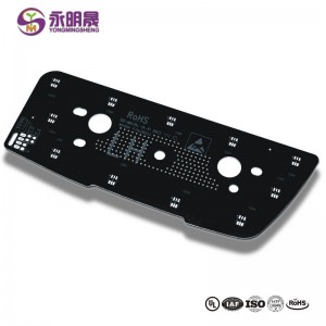
Gold finger is the connector at the edge of boards. It is similar to fingers, so we called gold finger, please see the following pictures. It is used to protect the printed circuit board prototypes from wear and tear.
The surface treatment of the gold finger PCB
Electroplated nickel gold: Thickness up to 3-50u", due to its superior conductivity, oxidation resistance and wear resistance, it is widely used in gold finger PCB that require frequent plugging or PCB комиссия that require frequent mechanical friction. While the cost of gold plating is extremely high, it is only applied to local gold plating such as gold fingers.
Immersion Gold: The thickness of conventional is 1u", up to 3u". It is widely used in high-precision PCB board with button position, bonded IC, BGA, etc. due to its superior conductivity, flatness and solderability. The gold finger PCB with low wear resistance requirements can also choose the entire board immersion gold process. The cost of the immersion gold process is much lower than that of the electric gold process. The color of the immersion gold process is golden yellow.
Goldfinger design in PCB
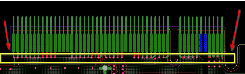
Goldfinger is an electrical interface. The common packaging form and appearance of PCB are as follows. When the appearance and packaging similar to the figure below are seen in the PCB design, the first reaction is to see them on the boardGold finger.
The easier way for goldfinger to judge is to have both the TOP and BOTTOM of the device
PIN device;It will look like the u-slot in the picture below.
When there is a goldfinger on the board, you need to work on the details of the goldfinger.
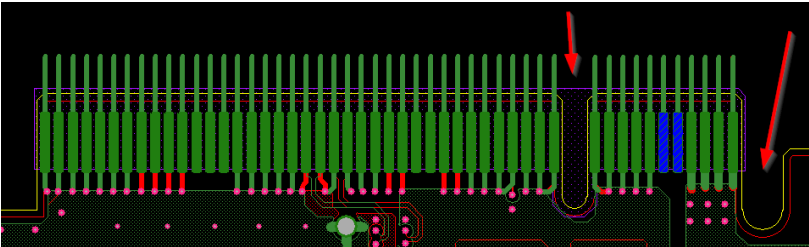
Details of goldfinger in PCB:
1) in order to increase the wear resistance of goldfinger, goldfinger usually needs to be plated with hard gold.
2) goldfinger needs chamfering, usually 45°, other angles such as 20°, 30°, etc.
If there is no chamfer in the design, there is a problem.In the figure below, the arrow is 45 degrees
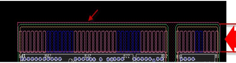
chamfering
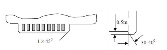
The 45° chamfering Angle in PCB is shown in the following figure:
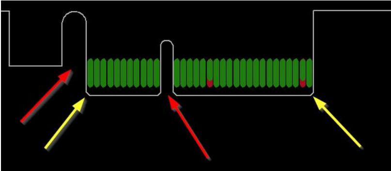
3) goldfinger needs to do the whole block of anti-welding window opening treatment, and the PIN does not need to open the steel net;
4) a minimum distance of 14mil from the tip of finger is required for the sink tin and silver welding pads;Recommended design
When the pad is more than 1mm away from the finger position, including the through hole pad;
5) do not coat goldfinger with copper;
Below is a goldfinger design for reference
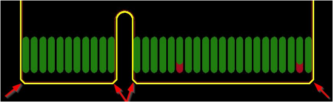
6) all layers of the inner layer of goldfinger need to be copper whittled, usually with a width of 3mm;
It can be done with half finger and whole finger.In pci-e design, there are also fingers
Remove all copper from the mingoldfinger area;
Goldfinger's resistance will be low, and cupping (hollowing out under the finger) will reduce it
The impedance difference between the impedance line and the impedance line is also beneficial to ESD.
Suggestion: cut all the copper under the goldfinger welding pad
YMS продуктулары жөнүндө көбүрөөк билүү
Көбүрөөк жаңылыктарды окуу

Products категориялар
-
FR4 Multilayer PCB-Chian Wholesale Supplier | Y...
-

LED дисплей экраны PCI HDI лазери аркылуу PAD копиясында ...
-
Калың жез PCB 10 катмар (4OZ) Жогорку Tg Толук B ...
-
PCB жылаңач тактай 4L Black Soldermask көмүлгөн тешик ...
-
оор жез PCB 4 Катмар (4/4/4 / 4OZ) Кара Сатылган ...
-

Wholesale Multi Layer PCB-PCB Manufacturer Chin...


