
 If you’re in a fast-moving industry, you need to know about high density interconnect PCB. Because some of your competitors are already start to use them.
High density interconnect PCBs are a way of making more room on your PCB to make them more efficient and allow for faster transmission. It’s relatively easy for most enterprising companies that are using printed circuit boards to see how this can benefit them.
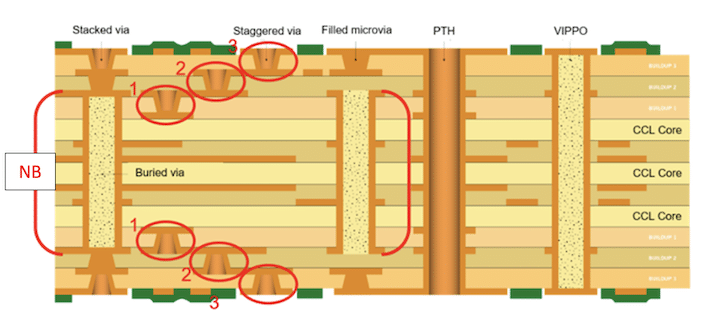
High density interconnect (HDI) PCBs represent one of the fastest-growing segments of the PCB market. Because of its higher circuitry density, the HDI technology can incorporate finer lines and spaces, smaller vias and capture pads, and higher connection pad densities. A high-density PCB features blind and buried vias and often contains microvias that are .006 in diameter or even less.
WHAT ARE HDI PRINTED CIRCUIT BOARDS?
HDI PCBs have a higher circuitry density per unit than conventional PCBs. They use a combination of buried and blind vias, as well as microvias — those that are 0.006″ or less in diameter. High-density circuit boards are PCBs with one or more of the following features:
Through vias and buried vias
Through vias from surface to surface
At least two layers with through vias
Coreless construction with layer pairs
Passive substrate constructions that have no electrical connection
Alternative constructions of coreless builds with layer pairs
What is the application of HDI PCB?
Healthcare
HDI PCBS are having an impact on the healthcare industry.Medical devices are often HDI because they can be packed in small devices like implants, LABS, and imaging equipment.Medical devices play a vital role in diagnosing disease and sustaining life.For example: pacemakers, diagnostic and monitoring equipment.With the miniaturized camera size, the patient’s internal parts can be observed to establish a correct diagnosis.Cameras are getting smaller, but picture quality is not affected at all.HDI PCB technology makes these advances possible.Cameras that need to be inserted at the open end, which some men find frustrating, are now smaller in size and clearer.I think the colonoscopy won’t hurt anymore.Thank God PCBS are shrinking or colonoscopies would keep patients away from them!
Automotive
Small PCBS are attractive to car manufacturers because they can save more interior space.Integrating electronics to provide a better driving experience has been a top focus for automakers as brands like Tesla roll out futuristic vehicles.Read Case Study: PCBS for Automotive Sensors.
Smartphones and Tablets
All smartphones are HDI PCBS with an ELIC(interconnect per layer) structure.HDI PCB is responsible for making thinner and smaller portable electronic devices.
Wearable Technology
With the introduction of wearable devices such as the Apple Watch and VR headsets, HDI is becoming a major stakeholder in the consumer market.This wearable technology is popular among young people because of its excellent features.
The Military and Aerospace
HDI is included in military communications equipment and other strategic equipment, such as missiles and defense systems.HDI PCBS are well suited for extreme environments and hazardous conditions, making them ideal for aerospace and military applications.
WHY CHOOSE YMS FOR YOUR HDI PCB?
YMS Circuits Limited has been delivering high-density interconnect printed circuit boards for more than 11 years, and we believe no order is too small, and no tolerance is too tight.Pair that with competitive pricing, quick quotes and response times, domestic and offshore manufacturing and an unprecedented level of flexibility, and you have a winning combination for all your HDI PCB needs.
Post time: Sep-09-2022