
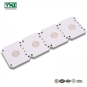
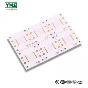
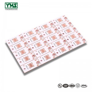
By copper coating, the unused space on the PCB is used as the base level and then filled with solid copper, which is also known as copper pouring.
The significance of copper coating lies in reducing ground resistance, improving anti-interference ability, reducing voltage drop, improving power efficiency, connecting to ground lines and reducing loop area.
Copper coating needs to pay attention to the following issues:
1.If there are more ground for PCB, such as SGND, AGND, GND, etc., the main "ground" shall be used as the reference for independent copper cladding according to the position of PCB board.
The digital ground and the analog ground separate to apply copper since not to say, at the same time before copper coating, first thicken the corresponding power line: 5.0v, 3.3v and so on, in this way, the formation of a number of different shapes of multi-deformation structure.
2.For different single point connections, the method is through 0 ohm resistance
3.Crystal oscillator: the crystal oscillator in the circuit is a high-frequency emission source. The method is to surround the crystal oscillator with copper, and then to ground the shell of the crystal oscillator separately.
4.The island (dead zone) problem, if it seems too big, is that defining a hole in the ground doesn't take much to add.
5.In the beginning of the wiring, should be equal to the ground wire, the wiring should be well, can not rely on copper through the addition of holes to eliminate the ground pin for connection, this effect is very bad.
6. It is better not to have sharp angle on the board (=180 degrees), because from the point of view of electromagnetism, this will constitute a transmitting antenna!
7.The wiring empty area of the middle layer of multilayer board, do not apply copper. Because it's hard for you to make this copper "well grounded."
8.The metal inside the equipment, such as metal radiator, metal reinforcement bar, must achieve "good grounding".
9.The backflow area of the three-terminal voltage regulator reduces the electromagnetic interference from the signal.
Searches related to PCB board
Post time: Sep-05-2019