
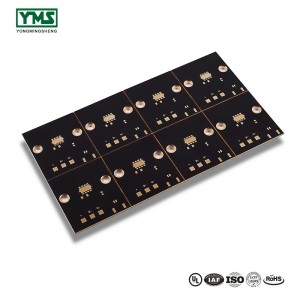
Copper coating is a common procedure that covers areas of a printed circuit board that are not wired with copper. This can enhance the anti-interference performance of the printed circuit board.
By copper coating, the unused space on the PCB is used as a base level and then filled with solid copper, which is also known as copper pouring.
Copper coating can reduce ground resistance, improve anti-interference ability, reduce voltage drop, improve power efficiency, in addition, it also connects with ground lines to reduce the loop area.
A. Copper coating needs to deal with several problems:
1. Different single point connection: the method is 0 ohm resistance or magnetic bead or inductance connection.
2. The copper coating near the crystal oscillator, the crystal oscillator in the circuit is a high-frequency emission source: the method is to surround the crystal oscillator with copper, and then the shell of the crystal oscillator is separately grounded.
3. Dead zone problem: if it feels big, it won't take much to define a hole and add it.
B. What are the benefits of copper cladding?
Improve power efficiency, reduce high-frequency interference, and another is to look beautiful!
Large area copper coating or mesh copper coating is good? Do not generalize. Why? Large area of copper coating, if the wave soldering, the plate may be up, or even blistering.
From this point, the mesh heat dissipation is better. Usually is the high frequency circuit to resist the interference request high multi-purpose grid, the low frequency circuit has the high current circuit and so on commonly complete copper coating.
In the beginning of the wiring, the ground wire should be treated equally, the wiring should be good, can not rely on copper coating through the addition of holes to eliminate the ground pin for connection, this effect is very bad.
Of course, if you choose the grid cladding, these lines will have some impact on the aesthetic, if it is careful to delete it.
Copper irrigation has intelligence, this operation will take the initiative to judge the network properties of the hole and the pad in the copper irrigation area, absolutely in line with the safe distance you set. This is different from drawing copper, which does not have this function.
Copper pouring has many functions. Pouring copper into the opposite side of the double panel and connecting it with ground noise can reduce interference, increase the laying range of ground wire and reduce low impedance, etc. Therefore, after the PCB wiring is basically completed, copper is often filled.
C. Copper clad wiring matters needing attention
1. PCB copper coating safety spacing setting:
The safe spacing of copper coating is generally two times that of wiring. However, in the absence of copper coating, the safe spacing of the wiring is set for the wiring, and then in the subsequent copper coating process, the safe spacing of the copper coating will default to the safe distance of the wiring. This is not the expected result.
One is to double the safe distance after the wire is laid, and then to copper cover, and then to change the safe distance back to the safe distance of the wiring after the copper cover, so that the DRC inspection will not report errors.
This method is ok, but if you want to change the copper coating again, you need to repeat the above steps, which is a little troublesome. The best way is to set the rules for the safe distance of the copper coating.
The other is to add rules.
In the Rule of the Clearance, to create a new Rule Clearance1 can customize (name), then :"Where the First Object matches" option box select the Advanced (Query), click the criteriabuilder, then appear "Building Query From Board" dialog box;
From the first drop-down menu in this dialog box, select the default "Show All Levels". From the ConditionType/Operator drop-down menu, select "Object Kind is".
This will display "Is Polygon" in "Query Preview", click OK, and when you're done, you'll get an error when you save completely:
Next, just change the "Is Polygon" to "In Polygon" in the "Full Query" display box, and then modify the desired copping spacing within Constraints.
Some people say that the priority of wiring rules is higher than the priority of copper-coating, copper-coating must follow the rules of safe spacing of wiring, need to add the copper-coating exception to the rules of safe spacing of wiring, the specific way is to note "not In Polygon" in the "Full Query".
There is no need to do this because the priority can be changed, there is an option in the lower left corner of the main page of the rule, priorities, to increase the priority of the copper-coated safe spacing rule to higher than the wiring safe spacing rule, so there is no interference.
2. PCB copper coated wire width setting:
Copper clad in choosing Hatched and None two modes, will note that there is a place set TrackWidth.
If you choose the default 8mil and the network you are copper clad to connect to has a minimum wire width of 8mil, then the DRC will report an error, not paying attention to this detail in the beginning, and there will be a lot of errors after each copper clad DRC.
In Rule Clearance, create a new Rule Clearance1 (name can be customized).
Then "Where the First Object matches" option box select the ADVANCED (Query), click the criteriabuilder, then appear "Building Query from Board" dialog box;
From the first drop-down menu in this dialog, select "Show All Levels" (by default), then ConditionType/Operator on "Object Kind is", and ConditionVALUE on the right on Ploy. This will display "Is Polygon" on the right "Query Preview". Click OK to save exit.
Now that we are done with this, change the "Is Polygon" to "In Polygon" in the "Full Query" display box. The final step is to modify the Constraints within the Constraints section.
In this way, it only affects the spacing of copper laying, not the spacing of each layer of wiring.
You May Like:
Post time: Sep-06-2019