
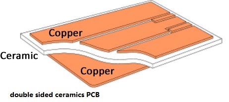
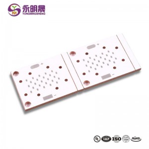
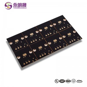
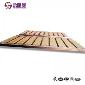
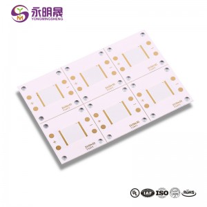
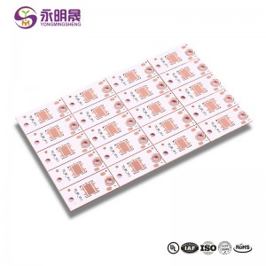
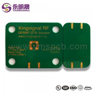
Ceramic PCB single and double sided ceramics PCB manufacture Ceramic Substrates| YMS PCB

Ceramic PCB: ceramic substrate circuit board
Ceramic Substrate describes a unique procedure board where the copper aluminum foil has straight adhered to the surface area (solitary side or dual side) of alumina (Al2O3) or lightweight aluminum nitride (AlN) ceramic substrate at heat. Compared to standard FR-4 or light weight aluminum substrate, the ultra-thin composite substrate made has exceptional electric insulation efficiency, high thermal conductivity, exceptional soft solderability and also high bond stamina, and also can be engraved numerous graphics like the PCB, with fantastic existing lugging ability. It appropriates for items with high warm generation (high-brightness LED, solar power), as well as its superb weather condition resistance is preferable for rough outside settings. Ceramic Circuit Board Technology Introduction
Why use ceramics material to produce circuit boards? Ceramic circuit boards are made of electronic ceramics and can be made in various shapes. The characteristics of high-temperature resistance and high electrical insulation of ceramic circuit boards are the most prominent. The advantages of low dielectric constant and dielectric loss, high thermal conductivity, good chemical stability, and similar thermal expansion coefficient to components are also significant. The production of ceramic circuit boards will use LAM technology, which is laser rapid activation metallization technology. They are used in the LED field, high-power power semiconductor modules, semiconductor refrigerators, electronic heaters, power control circuits, power hybrid circuits, smart power components, high-frequency switching power supplies, solid-state relays, automotive electronics, communications, aerospace, and military electronics components.
Advantages of Ceramic PCB
Unlike traditional FR-4, ceramic materials have good high-frequency performance and electrical performance, have high thermal conductivity, chemical stability, excellent thermal stability, and other properties that organic substrates do not have. It is a new ideal packaging material for the generation of large-scale integrated circuits and power electronic modules.
Main advantages:
Higher thermal conductivity.
More matching thermal expansion coefficient.
Stronger and lower resistance metal film alumina ceramic circuit board.
The solderability of the substrate is good, and the use temperature is high.
Good insulation.
Low high-frequency loss.
High-density assembly possible.
It does not contain organic ingredients, is resistant to cosmic rays, has high reliability in aerospace,and has a long service life.
The copper layer does not contain an oxide layer and can be used for a long time in a reducing atmosphere. Ceramic PCBs can be useful and efficient for printed circuit boards in these and many other industries, depending upon your design and manufacturing needs.
Ceramic PCB is a kind of heat conducting ceramic powder and organic binder, and the heat conduction organic ceramic PCB is prepared at a thermal conductivity of 9-20W/m. In other words, ceramic PCB is a printed circuit board with ceramic base material, which is highly thermally conductive materials such as alumina, aluminum nitride, as well as beryllium oxide, which can make a quick effect on transferring heat away from hot spots and dissipating it over the whole surface. What’s more, ceramic PCB is fabricated with LAM technology, which is a laser rapid activation metallization technology. So ceramic PCB is highly versatile that can take place of the entire traditional printed circuit board with a less complicated construction with enhanced performance.
Apart from MCPCB, if you want to use PCB in high pressure, high insulation, high frequency, high temperature, and high reliable and minor volume electronic products, then Ceramic PCB will be your best choice.
Why Ceramic PCB has such excellent performance? You can have a brief view on its basic structure and then you will understand.
- 96% or 98% Alumina (Al2O3), Aluminum Nitride (ALN), or Beryllium Oxide (BeO)
- Conductors material: For thin, thick film technology, it'll be silver palladium (AgPd), gold pllladium (AuPd); For DCB (Direct Copper Bonded) it'll be copper only
- Application temp: -55~850C
- Thermal conductivity value: 24W~28W/m-K (Al2O3); 150W~240W/m-K for ALN , 220~250W/m-K for BeO;
- Max compression strength: >7,000 N/cm2
- Breakdown Voltage (KV/mm): 15/20/28 for 0.25mm/0.63mm/1.0mm respectively
- Thermal expansion conefficient(ppm/K): 7.4 (under 50~200C)
Types of ceramic PCBs
1. High temperature ceramic PCB
2. Low temperature ceramic PCB
3.Thick film ceramic PCB
YMS Ceramic PCB manufacturing capabilities:
| YMS Ceramic PCB manufacturing capabilities overview | ||
| Feature | capabilities | |
| Layer Count | 1-2L | |
| Material and Thickness | Al203: 0.15, 0.38,0.5,0.635,1.0,1.5,2.0mm etc. | |
| SIN: 0.25,0.38,0.5,1.0mm etc. | ||
| AIN: 0.15, 0.25,0.38,0.5,1.0mm etc. | ||
| Thermal conductivity | Al203: Min. 24 W/m.k up to 30W/m.k | |
| SIN: Min. 85 W/m.k up to 100W/m.k | ||
| AIN: Min. 150 W/m.k up to 320 W/m.k | ||
| Al2O3 | Al2O3 has better light reflectivity - making it suited for LED products. | |
| SIN | SiN has a very low CTE. Coupled with a high Rupture Strength it can withstand stronger thermal shock. | |
| AlN | AlN has superior Thermal Conductivity - making it suitable for very high power applications requiring the best possible thermal substrate. | |
| Board Thickness | 0.25mm-3.0mm | |
| copper Thickness | 0.5-10OZ | |
| Minimum line Width and Space | 0.075mm/0.075mm(3mil/3mil) | |
| Speciality | Countersink,Counterbore drilling.etc. | |
| Min mechanical Drilled Size | 0.15mm(6mil) | |
| Conductors material: | For thin, thick film technology, it'll be silver palladium (AgPd), gold pllladium (AuPd),Platinum For DCB (Direct Copper Bonded) it'll be copper only | |
| Surface Finish | HASL, Lead free HASL,ENIG,Immersion Tin, OSP, Immersion Silver, Gold Finger, Electroplating Hard Gold, Selective OSP,ENEPIG.etc. | |
| Solder Mask | Green, Red, Yellow, Blue, White, Black, Purple, Matte Black, Matte green.etc. | |
| polished | Ra < 0.1 um | |
| lapped | Ra < 0.4 um | |
Learn more about YMS products
Read more news

Products categories
-
Metal clad pcb 1 Layer Thermoelectric Copper ba...
-
Thermal Clad metal core PCB Thermoelectric Copp...
-
Double sided metal core pcb Copper Base High Po...
-
Aluminum pcbs led aluminum pcb 1Layer mirror Al...
-
metal core pcb 1Layer Thermoelectric Copper bas...
-
Metal core PCB embedded copper coin pcb Thermal...


