
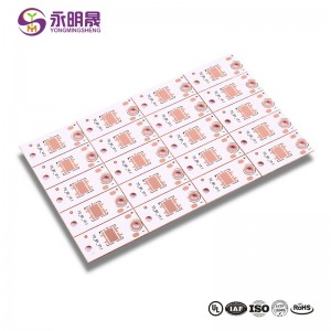
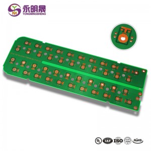
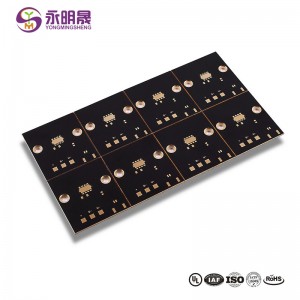
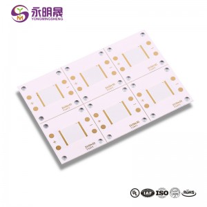
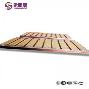
Metal clad pcb 1 Layer Thermoelectric Copper base Board| YMSPCB

YMS offers all the types of metal clad PCBs, and just contact us if you need thicker or thinner substrates. YMS will always keep our capabilities and equipment standards with the pace of advanced levels to provide customers with the best services of PCB prototype, PCB fabrication!
Parameters
- Layers: 1
- Thickness:2.0±0.15mm
- Base Material:copper alloy
- Min.Hole Size:0.5mm
- Minimum Line Width/Space:0.5mm/0.5mm
- Size:108mm×58mm
- Thermal Conductivity:4.0 W/mk
- Glass transition temperature: 170°C
- Surface treatment:Lead Free HASL
- Characteristics: High thermal conductivity
- Applications:LED
Copper base Board production process
- Provide the copper plate have pretreated
- UV ink is printed on the bending part of copper plate
- The surface of copper plate is browned by using browning liquid
- Press and drill copper plate covered with UV ink
- Electroplate the first finished product
- Make outer layer on copper plate
- Solder mask printing on copper substrate
- V – CUT the second finished product
- The bending position of copper plate is surface treated and the finished product is obtained
- Check up case ,packing and shipping
YMS copper based PCB manufacturing capabilities:
| YMS copper based PCB manufacturing capabilities overview | ||
| Feature | capabilities | |
| Layer Count | 1-4L | |
| Thermal Conductivity(w/m.k) | Aluminum PCB:0.8-10 | |
| Copper PCB:2.0-398 | ||
| Board Thickness | 0.4mm-5.0mm | |
| copper Thickness | 0.5-10OZ | |
| Minimum line Width and Space | 0.1mm/0.1mm(4mil/4mil) | |
| Speciality | Countersink,Counterbore drilling.etc. | |
| Types of Aluminum Substrates | 1000 series;5000 series;6000 series,3000 series.etc. | |
| Min mechanical Drilled Size | 0.2mm(8mil) | |
| Surface Finish | HASL, Lead free HASL,ENIG,Immersion Tin, OSP, Immersion Silver, Gold Finger, Electroplating Hard Gold, Selective OSP,ENEPIG.etc. | |
| Solder Mask | Green, Red, Yellow, Blue, White, Black, Purple, Matte Black, Matte green.etc. | |
You May Like:
1、PCB hole copper fracture reason
2、What are the requirements for copper thickness of PCB orifice
Learn more about YMS products

Write your message here and send it to us
Products categories
-
metal core pcb 1Layer Thermoelectric Copper bas...
-
Ceramic PCB single and double sided ceramics PC...
-
Thermal Clad metal core PCB Thermoelectric Copp...
-
Aluminum pcbs led aluminum pcb 1Layer mirror Al...
-
Metal core PCB embedded copper coin pcb Thermal...
-
Double sided metal core pcb Copper Base High Po...


