
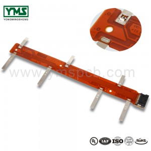
The Development of PCB Industry
PCB,the acronym of“Printed Circuit Board”, also known as PWB“PrintedWiring Board”, is made by graphic printing technology.It has replaced the way in which electrical products were made by copper wires before the 1940s,enabling large-scale and rapid production of products.The volume of products was reduced,the quality was stable, the production was convenient,and the unit price was reduced.
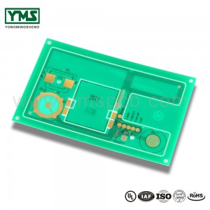
Early PCB has various features.Manufacturers used to make patterns on insulating plates by casting technology.After 1936, the manufacturing method turned to mental-covered insulating substrate,and manufacturers selectively used etching resist ink in different areas to remove unnecessary areas by etching.This technology was called“Subtractive Method”or“Print and Etch”process.
After 1960, the double-sided PCB with plated through-hole began to be used in phonograph,tape recorder and VCR.Epoxy with stable thermal resistance and good dimension performance has been widely used as the main resin material system for PCB, and has remained unchanged up to now.
Application of PCB
With the shift of industry from analog to digital, the mass production of PCB has been stimulated.From the radio,TV, tape recorder,to the walkman,calculators,computers,laptops,SPC exchange,mobilephones etc,they are all the examples.
Before, weused3C(Computer, Communication, Consumer Electronics) to define the PCB applications, but now with the highly development of electronic products, it'shard to do the same way already.
You May Like
Part of the information in our website is from the internet. If by any chance it violates your rights, we will delete it upon notification as soon as possible. Thank you for cooperation.
Post time: Jul-17-2020