
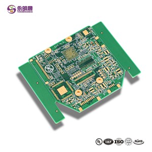
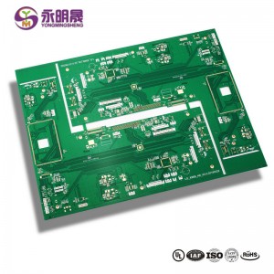
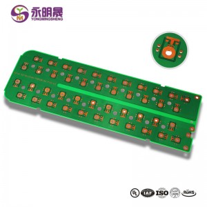
Metal pcb Double sided metal core pcb Metal clad pcb| YMS PCB

No ka mea hiki ke hooheheeia kūpapakū, ke keleawe a me ka Aluminum e ia i loko o PCB, akā, i likeʻole noi;
Eia naʻe, ina ua kamaʻilio aku ai, mai ka huina o ka PCB Plating, kiʻi mākou he ihola ia okoa pane:
PCB platingʻano nui mai nā 'keleawe, ke tina, nikala a me ke gula plating.Copper plating mea nui aaioee' enehana ma ka PCB manufacturing i.
E like me oe i ike, keleawe plating i na pono o ka maikai uila conductivity, thermal conductivity, me mechanical malleability, a no laila, ma luna,ʻo ia, keleawe kaiapuni ma hope oʻeli, electroplating o ka mea a pau PCB, a me ka hanaʻia naʻe kaapuni me ke keleawe, o ka a pau i e hōʻoia 'uila conductivity ; eia hou kekahi, ano o plating pāʻoihana o CuSO4;
In short, the process goes like this: drilling - immersion copper-plating - wire-drawing - etching
Makemake ʻoe:
1, Understand the construction of heavy copper PCB

Products waeʻano
-
OEM / ODM wale mai ana i pai ia Mana Lima huakai kaapuni a Papa M ...
-
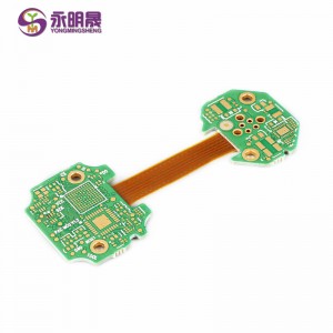
HDI Flex-Rigid Papa | ʻO YMS PCB
-
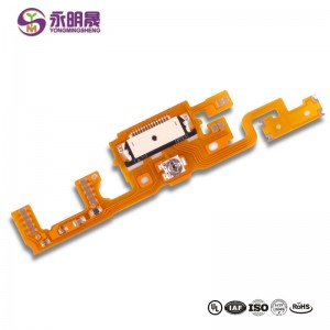
Flex Printed Circuit Board 1Layer | YMSPCB
-
ʻO ka wikiwiki kiʻekiʻe PCB POFV hoʻowalewale hoʻowalewale hōʻike enepig | ...
-
Kina 'Oihana Kina' Elevator Kaapuni PCB ...
-
Pālolo PCB hoʻokahi a pālua kapakahi keramika PC ...


