
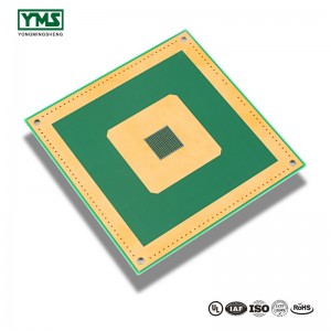
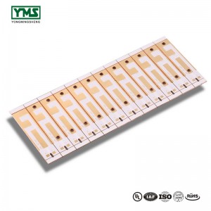
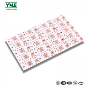
Heavy copper PCB is made with 4 or more ounces of copper per layer.
4 oz copper PCB is most commonly used in commercial products. Copper concentrations can be as high as 200 ounces per square foot.
Heavy copper PCB is widely used in electronics and circuits requiring high power transmission. In addition, the thermal strength provided by these PCBS is impeccable.
In many applications, especially electronics, the thermal range is critical because high temperatures can wreak havoc on sensitive electronic components and severely affect circuit performance.
The cooling capacity
Heavy copper PCB is much higher than casual PCB.
Cooling is critical to developing robust circuits. Improper thermal signal processing will not only affect the performance of electronic equipment, but also shorten the service life of the circuit.
Heavy copper PCB can be used to develop high power circuit wiring. This wiring mechanism provides more reliable thermal stress handling and provides fine machining while integrating multiple channels on a single compact plate.
Heavy copper PCB are widely used in a variety of products because they provide a variety of functions to improve circuit performance.
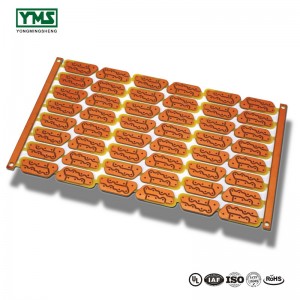
These PCBs are widely used in high-power equipment, such as transformers, radiators, inverters, military equipment, solar panels, automotive products, welding equipment and power distribution systems.
Heavy copper PCB manufacturing
As with standard PCB manufacturing, heavy copper PCB manufacturing, though, requires a lot more finicky processing.
The traditional heavy copper PCB is manufactured with outdated technology, which leads to uneven tracking and bottom cutting on the PCB, resulting in low efficiency. Today, however, modern manufacturing techniques support fine cutting and minimal bottom cutting.
Thermal stress treatment quality of heavy copper PCB
In designing circuits, factors such as thermal stress are very important and engineers should eliminate thermal stress as much as possible.
Over time, PCB manufacturing processes have evolved and various PCB technologies, such as aluminum base board, have been invented to handle thermal stress.
It is in the interest of heavy copper PCB designers to have thermal performance and environmental design that minimizes the power budget while maintaining the circuit.
As electronic components overheating can lead to failure, even life-threatening, hazard management can not be ignored.
The traditional technique for achieving heat dissipation quality is to use external heat sinks connected to the heating components. In order to dissipate this heat, the radiator consumes heat from the component and transmits it in the surrounding environment. Usually, these radiators are made of copper or aluminum. The use of these radiators not only exceeds the development cost, but also requires more space and time. Although the results are not even close to the heat dissipation capacity of heavy copper PCB.
In heavy copper PCB, the heat sink is built on the circuit board, instead of using any external heat sink. Since external radiators require more space, there are fewer restrictions on the placement of radiators.
Since the heat sink is electroplated on the circuit board and connected to the heat source using conductive through holes instead of any interface and mechanical joints, the heat transfer is rapid, thus improving the heat dissipation time.
Compared to other technologies, the cooling through-holes in heavy copper PCB can achieve more cooling, because the cooling through-holes are developed with copper. In addition, the current density was improved and the skin effect was minimized.
Advantages of heavy copper PCB
The advantages of heavy copper PCB make it the most important in the development of high power circuit.
Heavy copper concentrations can handle high power and heat, which is why high-power circuits have been developed using this technique. Such circuits cannot be developed with low-copper concentrated PCB because they cannot withstand the huge thermal stress caused by high current and flow current. Heavy copper PCB is generally considered to be high current PCB because of its significant heat dissipation capability.
The relationship between PCB copper thickness and current is an important factor in using heavy copper PCB. As the copper concentration increases, so does the total cross-sectional area of the copper, which reduces the resistance in the circuit. As we know, losses are devastating to any design, and copper concentrations allow these PCB's to reduce power budgets.
Current conductivity is an important factor, especially when dealing with low power signals, and when using heavy copper PCB, the current conductivity is improved by its minimal resistance.
Connectors are essential when connecting jumpers. However, connectors are often difficult to maintain on traditional PCB. Connectors are usually affected by mechanical stress due to the low strength of occasional PCB, but heavy copper PCB provides higher strength, ensuring higher reliability.
YONGMINGSHENG heavy copper PCB manufacturing
Heavy copper PCB manufacturing requires proper care, and improper handling in the manufacturing process can lead to poor performance. Always consider the services of an experienced manufacturer.
YONGMINGSHENG provides execution PCB manufacturing facilities for all types of PCB. We focus on heavy copper PCB manufacturing and develop high quality production images.
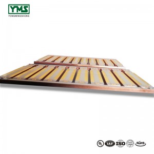
Heavy copper PCB is manufactured on advanced automation machines, which allows us to develop highly reliable PCB. So far, we have developed two-layer PCB, up to 20 ounces, multi-layer PCB, copper weight 4-6 ounces.
You May Like:
Post time: Sep-06-2019