
Can PCB copper thickness be controlled in software?
This is the first time I've heard of it. Even if there are PCB manufacturers, they will not look at this project, because there is no routine operation like this. The thickness is not increased by software, and it is customized to the manufacturer.
If you want to control the copper thickness of PCB, it is good to write the requirements clearly, let the PCB manufacturer according to your requirements to make to control the copper thickness of the line. You just need to say it with the manufacturer of the board, but it seems that it is not as much as you want, and there is also upper limit value. At present, the largest one I know is only 100um.
How to achieve the copper thickness of the heavy copper board
Heavy copper board because of PCB usage and signal current size thickness and different, the copper thickness of heavy copper board is how to achieve the production?
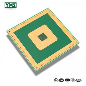
In the printed circuit board industry, there is no clear definition of heavy copper board. Generally speaking, the board with copper thickness≥2oz is called heavy copper board.
Most printed circuit boards use 35um copper foil thickness, which depends on PCB usage and signal voltage/current. For PCB with excessive current, 70um copper thickness will be used, 105um copper thickness will be used, and 140um copper thickness will be rarely used.
The copper thickness of heavy copper board is how to achieve? Generally, the finished copper thickness of 2oz is not enough to fill the ravages between the lines with one screen printing by hand, so the resistance welding must be printed twice.
Therefore, when the printed circuit board is produced, it is generally encountered with 2oz and thicker, and it will be noted during the resistance welding: heavy copper board, which needs second screen printing. In order to achieve the line is not red, line surface resistance welding thickness is greater than 10um.
The hole copper of the printed circuit board is not as thick as possible, all the data need to be made according to the requirements of the customer. Customer requirements to achieve as much as possible, naturally this can not be completely consistent, but must be within the customer allowed error.
Copper plating usually includes primary copper and secondary copper. The main purpose of primary copper is to provide sufficient copper thickness for secondary copper etching, so as to ensure that the copper thickness after secondary copper etching can meet customer's standard requirements.
Heavy copper board can process 6oz, 3oz, 2oz thick copper plate, generally need multilayer screen printing and multilayer solder resistance and multilayer copper deposition, to meet customer needs.
You May Like:
Post time: Sep-11-2019