
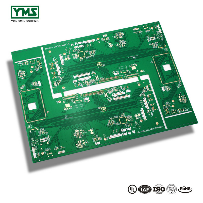
PCB (printed circuit board) can be divided into Rigid PCB and Fexible PCB, the former can be divided into three types: single-layer PCB, double-layer PCB and multi-layer PCB.
According to the quality grade, PCB can be divided into three quality grades: 1, 2 and 3, among which 3 have the highest requirements. Differences in PCB quality levels lead to differences in complexity and testing and inspection methods.
So far, rigid double-layer and multi-layer PCBs have made up a relatively large portion of applications in electronics, and sometimes using flexible PCBs in some cases. Therefore, this paper will focus on the rigid double-layer and multi-layer PCB quality testing.
After PCB manufacture, inspection must be carried out to determine if the quality is compatible with the design requirements. It can be considered that quality inspection is an important guarantee of product quality and the smooth implementation of follow-up procedures.
Inspection standard
PCB board inspection standards mainly include the following aspects:
A. Standards set by each country;
B. Military standards for each country;
C. Industrial standards such as SJ/T10309;
D. PCB inspection instructions prepared by equipment supplier;
E. Technical requirements on PCB design drawings.
For PCBS that have been identified as keyboards in the device, these key characteristic parameters and metrics must be focused and checked from the head in addition to regular inspection
Inspection items
Regardless of the type of PCB, they must go through similar quality inspection methods and items. According to the inspection method, the quality inspection items usually include visual inspection, general electrical performance inspection, general technical performance inspection and metallization inspection.
• visual inspection
Visual inspection is easy with the help of a ruler, a vernier caliper, or a magnifying glass. The inspection includes:
A. Plate thickness, surface roughness and warping.
B. Appearance and assembly dimensions, especially those compatible with electrical connectors and rails.
C. Conductive pattern integrity and clarity as well as the presence of bridged short circuits, open circuits, burrs or voids.
D. The quality of the surface of a print line or pad, the presence of pits, scratches, or pinholes. Weld pad through hole and other through hole positions.The hole should be checked for missing or incorrect punching, whether the diameter of the through hole is in accordance with the design requirements and whether there are nodules and gaps.
F. Pad quality and firmness, roughness, brightness and gaps in raised defects.
G. Coating quality.The coating flux is uniform and firm, the position is correct, the flux is uniform, the color is in accordance with the requirements.
H. Character qualities, such as whether they are firm, clean and clean, without scratches, penetration or disconnection.
• general electrical performance inspection
There are two tests under this type of inspection:
A. Connection performance testing. In this test, the multimeter is usually used to check the connectivity of the conductive pattern through the focusing metallized through-hole of the double-layer PCB and the connection performance of the multi-layer PCB. For this test, PCBCart provides a general inspection before each manufactured PCB leaves its warehouse to ensure the implementation of its basic functions.
B. Insulating performancetest. The purpose of this test is to check the insulation resistance of the same plane or between different planes to ensure the insulation performance of the PCB.
• general technical inspection
General technical inspection includes weldability and plating adhesion inspection. For the former, check the wettability of the solder to the conductive pattern. For the latter, it can be checked by qualified tips, which are first glued to the electroplating surface to be examined and then pulled out quickly after being pressed evenly.
Next, the plating plane should be observed to ensure that no shedding occurs. In addition, according to the actual situation to choose some inspection, such as copper foil anti-fall strength and metallized anti-tensile strength.
• metallization by inspection
The quality of metallized through-hole plays an important role in double-layer PCB and multi-layer PCB. A large number of failures of electrical modules and even the whole equipment are due to the quality of metallized holes. Therefore, it is necessary to pay more attention to the inspection of metallized holes. Metallization inspection includes the following aspects:
A. The metal plane of the through hole wall shall be complete, smooth, and void or nodule.
B. Electrical property inspection shall be carried out in accordance with the short-circuit and open circuit of the pad and the resistance between the through hole and the lead through the metallization of the plating plane.
After the environmental test, the resistance change rate through the hole should not exceed 5% to 10%. Mechanical strength refers to the bonding strength between the metallized through hole and the pad.
The metallographic analysis test is responsible for checking the quality of the plating plane, the thickness and evenness of the plating plane, and the bonding strength between the plating plane and the copper foil.
Metallization tests are usually combined with visual and mechanical tests. Visual inspection is to observe that the PCB is placed in the light and the complete smooth through hole wall can reflect the light evenly.
However, the wall through which the nodules or Spaces are contained will not be so bright. For mass production, the inspection should be carried out by the flying needle tester and other online testing equipment.
Due to the complex structure of multi-layer PCB, it is difficult to quickly locate the fault in the subsequent assembly and test of unit modules once there is a problem. Therefore, the quality and reliability of the inspection must be very strict.
In addition to the above routine inspection items, other inspection items include the following parameters: conductor resistance, metalized through-hole resistance, inner layer short circuit and open circuit, insulation resistance between wires, plating plane adhesion strength, adhesion, thermal shock resistance, shock resistance, mechanical shock, current strength, etc. Each indicator must be obtained through the application of specialized equipment and methods.
Post time: Oct-29-2019