
Copper-clad, in which unused space on a PCB board is used as a base level and then filled with solid copper, also known as copper filler.
The significance of copper coating lies in reducing ground resistance and improving anti-interference ability; reduce voltage drop, improve power efficiency; and also, connect to ground lines, reduce loop area.
If there are many PCB places, such as SGND, AGND, GND, etc., how to cover copper?
In my practice, according to the position of PCB board, the main "ground" is used as the reference for independent copper coating, and the DGND and AGND are separate used for copper coating.At the same time, before copper coating, first bold the corresponding power line: v5.0v, v3.6v, v3.3v (SD card power supply), etc.In this way, multiple deformation structures of different shapes are formed.
Copper coating needs to deal with several issues:
1. Different single point connections;
2. For the copper coating near the crystal oscillator, the crystal oscillator in the circuit is a high-frequency emission source. The method is to apply copper around the crystal oscillator, and then ground the shell of the crystal oscillator separately.
3. The island (dead zone) problem, if it feels very big, it dosen't take much to define a hole in the ground and add it.
In addition, a large area of copper cladding is good or grid copper cladding, not to generalize. Why?
Large area of copper coating, if the wave soldering, the plate may be up, or even blistering.From this point, the mesh heat dissipation is better.
Usually is the high frequency circuit to resist the interference request high multi-purpose grid, the low frequency circuit has the high current circuit and so on commonly complete copper coating.
Yongmingsheng is a China PCB manufacturer. Our products include: Single layer PCB, double layer PCB, multi-layer PCB; welcome to consult !
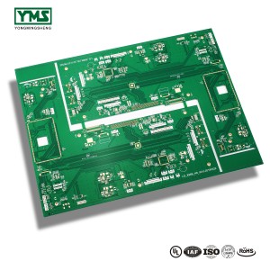
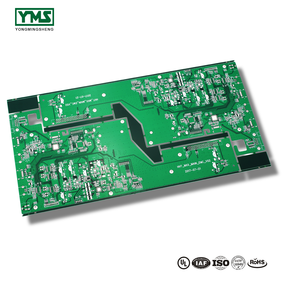
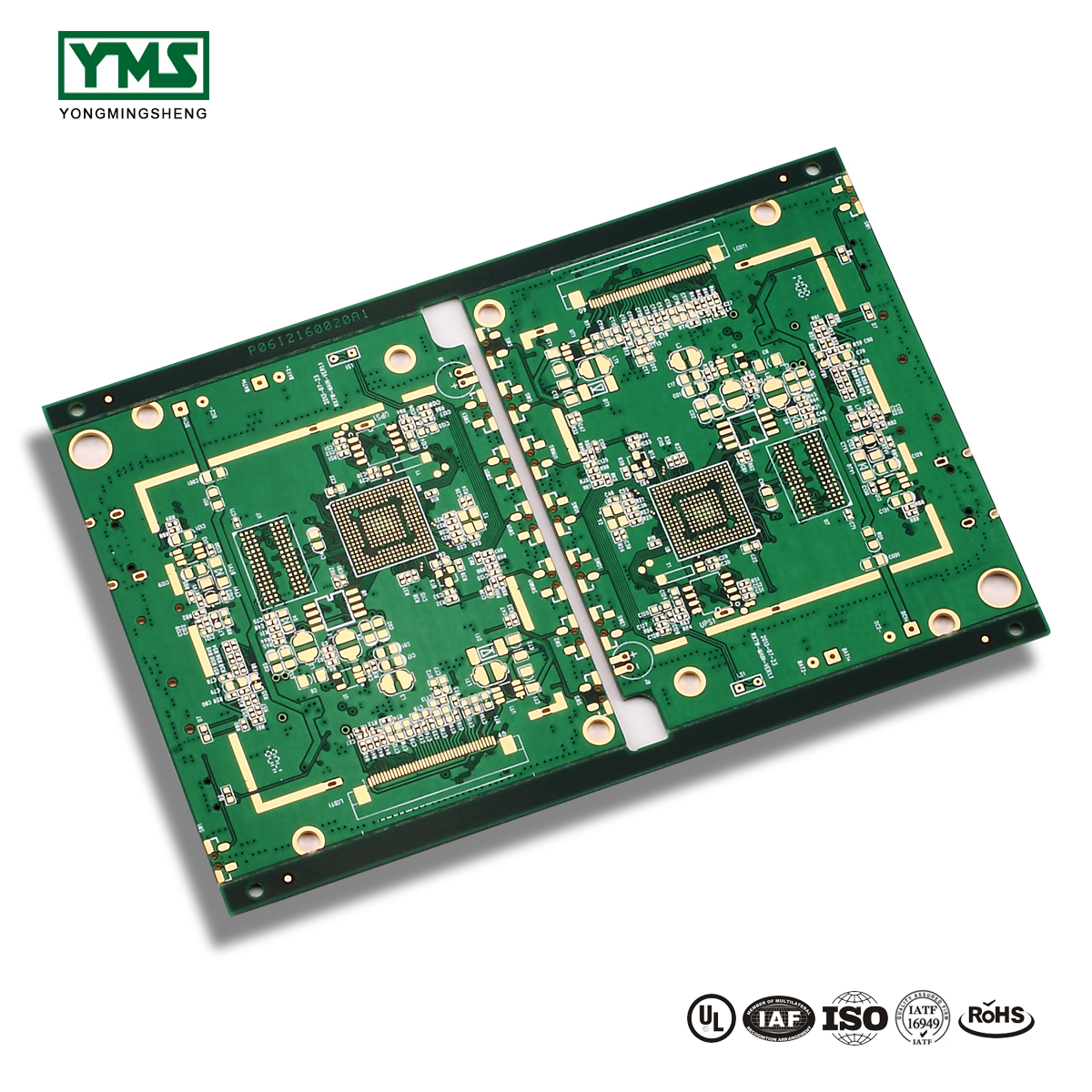
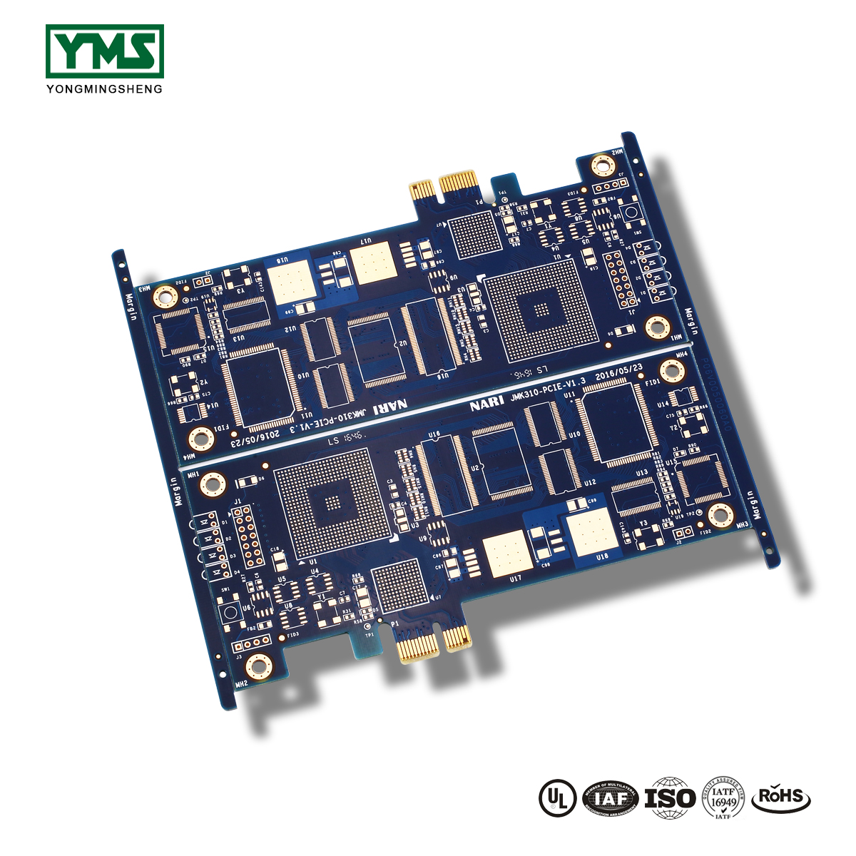
PCB Circuit Board
Post time: Aug-17-2019