
Gold Finger
On computer memory sticks and video CARDS, we can see a row of golden conductive contacts. They are called “gold fingers“.
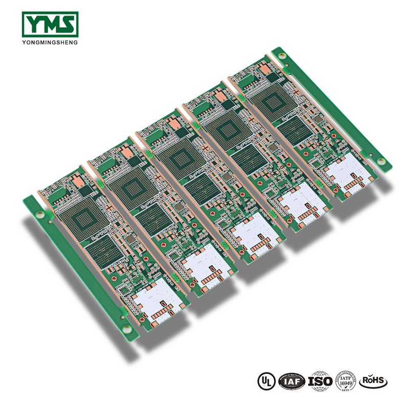
The Gold Finger (or Edge Connector) in the PCB design and manufacture industry uses the Connector as the outlet of the board to the external connection network.
Next, let’s take a look at the processing of goldfinger in PCB and some details.
Goldfinger PCB surface treatment
1. Nickel gold plating:
Thickness up to 3-50u “, due to its superior electrical conductivity, oxidation resistance and wear resistance, it is widely used on the goldfinger PCB that needs to be inserted frequently or on the PCB board that needs to be rubbed frequently, but because of the high cost of gold plating, it is only used on the local gold plating treatment such as goldfinger.
2. Gold deposit:
Thickness of conventional 1u “, up to 3u “due to its superior conductivity, smoothness and weldability, has been widely used in the design of button position, binding IC, BGA and other high precision PCB, for the wear-resistance requirements are not high goldfinger PCB, you can also choose the whole plate sinking process, sinking process cost is much lower than the electrogold process cost. The color of sinter is golden.
PCB gold finger details processing
(1) To increase the wear resistance of goldfinger, it is usually necessary to electroplate hard gold.
(2) Gold finger needs chamfer, usually 45°, other angles such as 20°, 30°, etc. If there is no chamfer in the design, there is a problem.
(3) The golden finger needs to do the whole block blocking welding window opening, and the PIN does not need to open the steel mesh.
(4) The minimum distance between the solder pad and the tip of the finger is 14mil; It is recommended that the pad should be more than 1mm away from the finger position during design, including the through-hole pad.
(5) Do not cover the gold finger with copper.
(6) All layers of the inner layer of the golden finger need to be processed with copper cutting, and the width of copper cutting is usually 3mm larger. Can do half finger copper and the whole finger copper.
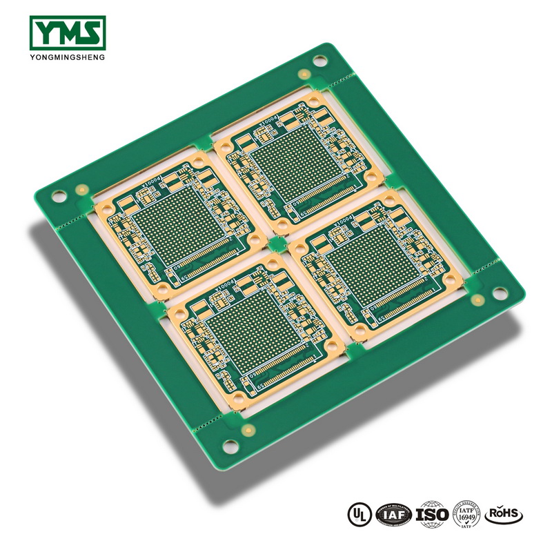
Yongmingsheng technology co., LTD. is a high-tech company integrating circuit board development, design, proofing, production (processing), testing, production and sales.
The main products are:PCB gold finger,flexible rinted circuit board,flex-rigid,reasonable price;
Since the establishment of the company, from the original professional circuit board processing, to expand the production of flexible circuit board, rigid circuit board, etc. We have been making progress, we have been committed to become a high quality PCB manufacturer and service provider.
Post time: Sep-19-2019