
Using different resin systems and substrate materials, different resin systems will lead to significant differences in the activation effect of copper deposition and copper deposition.
In particular, some CEM composite substrate and high-frequency plate silver substrate specificity, when doing the chemical copper treatment, need to take some special methods, if the normal chemical copper is difficult to achieve good results.
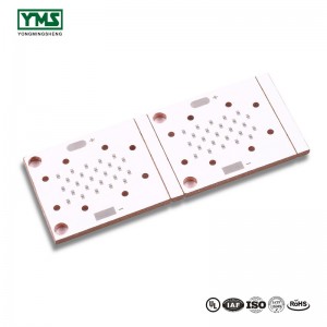
Base board pre - treatment problem.
Some substrates may absorb moisture and itself in the pressure of synthetic substrates when partial resin curing bad, so when drilling may not be enough because of resin itself strength and cause drilling quality is very poor, drilling pollution or hole wall resin tear dig serious etc., so when cutting materials necessary baking should be.
In addition, some multi-layer board may also appear after lamination pp semi-solidified substrate area branch curing bad condition, also will directly affect drilling and rubber residue activation copper deposition.
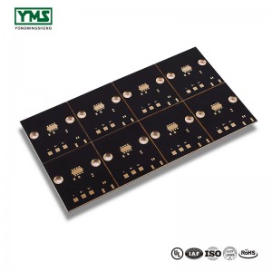
The drilling condition is too bad, mainly manifested as: there is much resin dust in the hole, the wall of the hole is rough, the burr in the hole is serious, the burr in the hole, the inner copper foil nail head, the tear section length of the glass fiber area is not uniform, etc., all of which will cause certain quality hazards to the chemical copper.
In addition to mechanically removing surface contamination from the substrate and removing burrs/burrs from the orifice, the brush plate cleans the surface and, in many cases, cleans and removes dust from the orifice.In particular, more than a few do not go through the process of degumming residue treatment of the double panel is more important.
Another point to note, do not think that the removal of rubber residue can be out of the hole in the rubber residue and dust, in fact, in many cases, the removal of rubber residue technology dust treatment effect is very limited;
Because the dust in the bath will form small micelles, making the bath difficult to deal with, this micelle adsorbed on the wall of the hole may form the plating tumor in the hole, or it may fall off from the wall of the hole in the subsequent processing, which may also cause the point in the hole without copper;
Therefore, for multi-layer board and double-layer board, the necessary mechanical brush board and high pressure cleaning is also necessary, especially facing the industry development trend, hole board and high aspect ratio board is more and more common. Even sometimes ultrasonic cleaning to remove dust in the hole has become a trend.
There are no copper holes caused by nothing more than:
1. Dust plug hole or hole thickness.
2. When sinking copper potions have bubbles, the hole did not sink copper.
3. There is line ink in the hole, no electric protective layer, no copper in the hole after etching.
4. The acid and alkali solution in the hole after copper sinking or plate electricity is not cleaned, and the parking time is too long, resulting in slow bite corrosion.
5. Improper operation, too long stay in the process of micro corrosion.
6. If the punching plate pressure is too high, (the designed punching hole is too close to the conductive hole), the middle part should be disconnected neatly.
7. Poor permeability of electroplating potions (tin, nickel).
To improve the causes of the 7 major problems of producing holes without copper:
1. Add high-pressure washing and rubber residue removal procedures to the holes prone to dust (such as 0.3mm in the diameter below 0.3mm).
2. Improve the activity and shock effect of the potion.
3. Change the printing screen plate and counterpoint film.
4. Extend the washing time and specify how many hours to complete the pattern transfer.
5.Set a timer.
6. Add explosion-proof holes.Reduce the force on the plate.
7. Do regular penetration tests.
You May Like:
Post time: Sep-04-2019