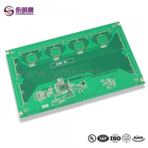
High speed PCB POFV insertion loss test enepig| YMSPCB

What is a High Speed PCB?
"High Speed" is generally interpreted to mean circuits where the length of the signal's rising or falling edge is greater than about one-sixth of the transmission line length greater then the transmission line length, then the transmission line length demonstrates lumped line behavior.
In a high speed PCB, the rise time is fast enough that the bandwidth for the digital signal can extend into the high MHz or GHz frequencies. When this happens, there are certain signalling problems that will be noticed if a board is not designed using high speed PCB design rules. In particular, one might notice:
1. Unacceptably large transient ringing. This generally occurs when traces are not wide enough, although you need to be careful when making your traces wider (see the section on Impedance Contorl in PCB Design below). If transient ringing is quite large, you'll have large overshoot or undershoot in your signal transitions.
2.Strong crosstalk. As the signal speed increases (i.e., as the rise time decreases), capacitive crosstalk can become quite large as the induced current experiences capacitive impedance.
3.Reflections off of driver and receiver components. Your signals can reflect off of other components whenever there is an impedance mismatch. Whether or not the impedance mismatch becomes important requires looking at the input impedance, load impedance, and transmission line characteristic impedance for an interconnect. You can read more about this in the following section.
4.Power integrity problems (transient PDN ripple, ground bounce, etc.). This is another set of unavoidable problems in any design. However, transient PDN ripple and any resulting EMI can be reduced significantly through proper stackup design and decoupling measures. You can read more about high speed PCB stackup design later in this guide.
5.Strong conducted and radiated EMI. The study of solving EMI problems is extensive, both at the IC level and the high speed PCB design level. EMI is essentially a reciprocal process; if you design your board to have strong EMI immunity, then it will emit less EMI. Again, most of this boils down to designing the right PCB stackup.
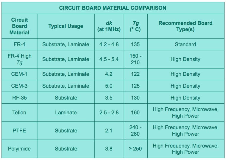
High-frequency PCBs usually provide a frequency range from 500MHz to 2 GHz, which can meet the needs of high-speed PCB designs, microwave, radiofrequency, and mobile applications. When the frequency is above 1 GHz, we can define it as high frequency.
The complexity of electronic components and switches is continually increasing nowadays and need faster signal flow rates. So, higher transmission frequencies are required. High-frequency PCBs help a lot when integrating special signal requirements into electronic components and products with advantages like high efficiency, and fast speed, lower attenuation, and constant dielectric properties.Some considerations of high-frequency PCBs designs
High-frequency PCBs are mainly used in radio and high-speed digital applications, such as 5G wireless communications, automotive radar sensors, aerospace, satellites, etc. But there are many important factors to be considered when manufacturing high-frequency PCBs.
· Multi-layered design
We usually use multi-layered PCBs in high-frequency PCB designs. Multi-layered PCBs have assembly density and small volume, making them very suitable for impact packages. And multi-layered boards are convenient to shorten the connections between electronic components and improve the speed of signal transmission.
Ground plane designing is an important part of high-frequency applications because it not only maintains signal quality but also helps reduce EMI radiations.High frequency board for wireless applications and data rates in the upper GHz range have special demands on the material used:
1. Adapted permittivity.
2.Low attenuation for efficient signal transmission.
3.Homogeneous construction with low tolerances in insulation thickness and dielectric constant. The demand for high-frequency and high-speed PCB products rises rapidly nowadays. As an experienced produttore di PCB , YMS is focusing on providing customers with reliable high-frequency PCB prototyping with high quality. If you have any problems with PCB designing or PCB manufacturing, please feel free to contact us.
| YMS High Speed PCB manufacturing capabilities overview | ||
| Caratteristica | capacità | |
| Conteggio strati | 2-30L | |
| Available Alta velocità PCB Technology | Foro passante con rapporto di aspetto 16: 1 | |
| sepolto e cieco via | ||
| Mixed Dielectric Boards (High Speed Materiale+FR-4 combinations ) | ||
| Suitable Alta velocità Materials available : M4,M6 series,N4000-13 series, FR408HR,TU862HFTU872SLKSP, EM828,etc. | ||
| Tight Etch Tolerances on Critical RF Features:+/- .0005″ standard tolerance for unplated 0.5oz copper | ||
| Multilevel cavity constructions, Copper coins and slugs, Metal Core & Metal Back, Thermally conductive laminates,Edge Plating, etc. | ||
| Spessore | 0,3 mm-8 mm | |
| Larghezza e spazio minimo della linea | 0,075 mm/0,075 mm (3 mil/3 mil) | |
| PASSO BGA | 0,35 mm | |
| Dimensione min forata laser | 0,075 mm (3 a zero) | |
| Dimensione minima forata meccanica | 0,15 mm (6 mil) | |
| Proporzioni per foro laser | 0.9: 1 | |
| Rapporto d'aspetto per foro passante | 16: 1 | |
| Finitura superficiale | Suitable Alta velocità PCB urface finishes: Electroless Nickel, Immersion Gold, ENEPIG, Lead free HASL,Immersion Silver | |
| Tramite l'opzione di riempimento | Il via è placcato e riempito con resina epossidica conduttiva o non conduttiva, quindi tappato e placcato (VIPPO) | |
| Riempito di rame, riempito d'argento | ||
| Laser via rame placcato chiuso | ||
| Registrazione | ± 4mil | |
| Maschera per saldatura | Verde, rosso, giallo, blu, bianco, nero, viola, nero opaco, green.etc opaco. | |
Scopri di più sui prodotti YMS
video