
This article is mainly PCB manufacturers tell you heavy copper board wiring what are the precautions? I hope I can help you.
1. 3 points above the line, try to let the line through each point in turn, easy to test, the line length as short as possible.
2. Do not lay wires between pins, especially between and around pins of integrated circuit.
3. The lines between different layers should not be parallel as far as possible to avoid the formation of actual capacitance.
4. Wiring as far as possible is a straight line, or 45 degrees broken line, to avoid the generation of electromagnetic radiation.
5. At least 10-15mil of ground wire and power wire (for logic circuit).
6. Try to connect the polysemous wires to increase the grounding area. Line to line as neat as possible.
7. Pay attention to the uniform distribution of components, for installation, plug-in, welding operation. The text is arranged in the current character layer, with reasonable position, attention to orientation, to avoid being blocked, so as to facilitate production.
8. Take the structure into consideration. The positive and negative poles of the patch elements should be marked in the package and at the end to avoid space conflicts.
9. At present, PCB can be used for wiring of 4-5mil, but it is usually used for 6mil wire width, 8mil wire distance, 12/20mil welding pad. Wiring should take into account the effect of filling current, etc.
10. The functional block elements should be put together as far as possible, zebra bar and other elements near the LCD should not be too close.
11. Through the hole to apply green oil (set as a negative double value).
12. It is better not to place welding PAD or overempty PAD under the battery holder. PAD and VIL are reasonable in size.
13. Check carefully whether each cable (including NETLABLE) is actually connected (with the light-up method) after wiring is completed.
14. Oscillating circuit elements should be close to IC as far as possible, and oscillating circuit should be far from antenna and other vulnerable interference areas. Grounding pad should be put under crystal vibration.
15. Consider reinforcement, hollowing and other ways to avoid excessive radiation sources.
Conclusion: the two intermediate layers of the four layers PCB are actually used as the power layer and the stratum. Please pay attention to the arrangement of the power source and the ground plane. The power source and the ground are connected with the power source and the ground plane through holes nearby.
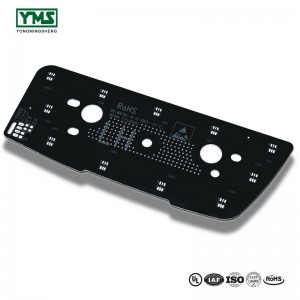
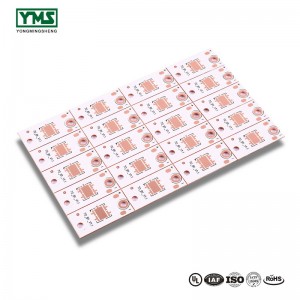
Yongmingsheng technology co., LTD. is a high-tech company integrating circuit board development, design, proofing, production (processing), testing, production and sales.
The main products are: flexible board, flex-rigid ,metal PCB, reasonable price;
Since the establishment of the company, from the original professional circuit board processing, to expand the production of flexible circuit board, rigid circuit board, etc. We have been making progress, we have been committed to become a high quality PCB manufacturer and service provider.
You May Like:

Post time: Sep-16-2019