
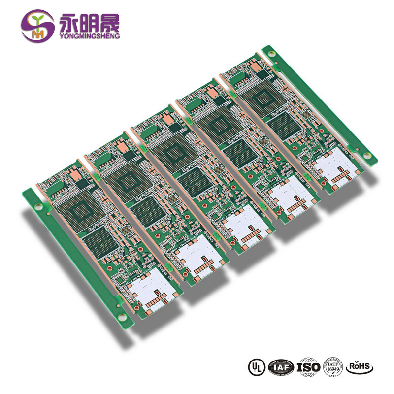
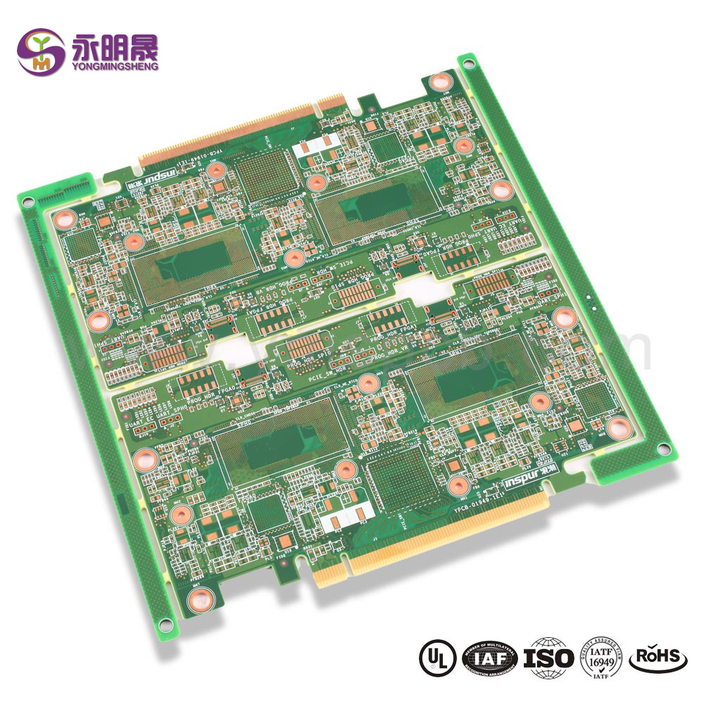
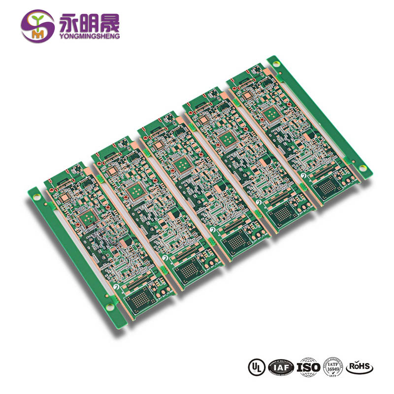
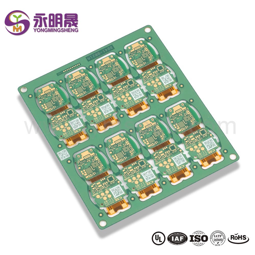
HDI PCB is the high-density interconnector PCB. It is a type of PCB technology that is very popular in various devices. HDI PCBs are the results of miniaturization of components and semiconductor packages because they can realize more functions on the same or less board area through some technologies.
Explicitly, with these technology growths, and within, the new questions will come up regarding the process underlying the actual these boards manufacture. These boards tolerances must be right on the denser of your parts. Parts like annular rings, drilling, routing, lamination cycles, and soldering would all can be produced to obtain desired outcomes. Recalling our rainbow cake, manufacturing is quite the same with that in theory. Moreover, the more number of layers we want to extent also the more routing plans in internal we present, the more complex the fabrication machines have to be.
It is like a baker’s cleanroom that needs the utilization of lab coats in vacuumsealed condition, laser imaging equipments, and also high-tech covering stations now where I would like to look at a cake.The efforts and cost related to producing these PCBs can easily overbalance the advantages, although also can fairly be justified. Because it merely depends on the applications. Developing a radio device for kids would probably not confirm these costs. Developing a jammer using RF signal with military-grade to be put in a fighter aircraft?
Maybe you should consider it. Whatever the application may be, remember that the extra processes and equipment required to manufacture these HDI PCBs and would be a big aspect at play.
HDI PCB is just one of the solutions being used to fit the growth requests of the consumer expectations. Using vias to cope smart pad processes and routing plans can obtain unheard of various densities in the today’s devices. As the growth in technology, of course, implies the increase in expense, however with the total of effort
and time already initiated at the arena, fabrication expenses could be assessed to start to even up and immerse into the hobbyist accessibility.
The birth of the HDI PCBs brings more possibilities for portable electronic devices and more challenges for PCB manufacturers. For accommodating the trend of miniaturization and multifunction of electronics, YMS has done a lot to improve the level of equipment and staff professionalism.
You can be assured to offer us the HDI designs, and we will give you a satisfactory service and HDI products.
Learn more about YMS products
Post time: Nov-09-2021