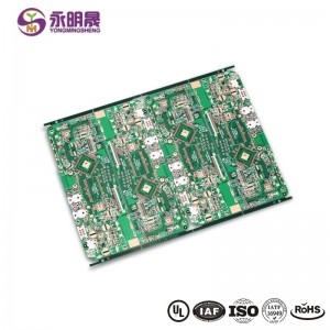
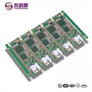
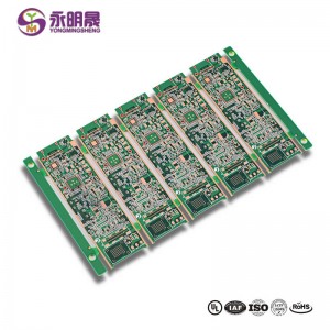
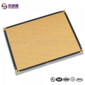
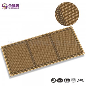
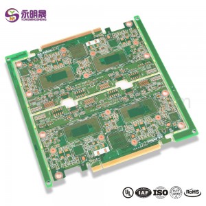
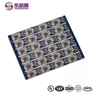
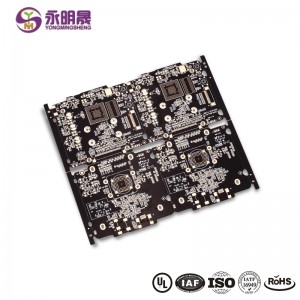
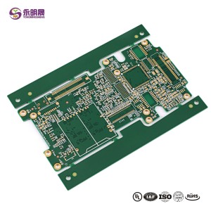
High-density interconnect (HDI) printed circuit boards (PCBs) are an increasingly integral part of the PCB and electronics industries. Electronic components are becoming smaller and more lightweight but still demand ever-improving performance. To accommodate this, you need to pack more functionality into a smaller area. That’s precisely what HDI PCBs offer.
Over the course of a decade in business, YMSPCB has established a hard-earned reputation for manufacturing PCBs of the highest quality. Our custom PCB manufacturing capabilities enable you to get the finest quality HDI PCBs at competitive prices without min order quantity requirement. Our team run design for manufacture check on your custom PCB file and consult with you to ensure it is ready for manufacturing and that your boards will meet your performance requirements. We also have an on-site quality control department to verify the finished product meet your high quality standards.
