
1. How to choose EDA things
In current PCB planning software, thermal analysis is not a strong point, so it is not recommended to choose. Other functions 1.3.4 can select PADS or Cadence with good performance and price.
PLD planning beginners can choose the integrated environment provided by the PLD chip manufacturers, to achieve more than a million door planning can choose a single thing.
2. Please introduce a suitable for high-speed signal processing and transmission EDA software.
Conventional circuit planning, INNOVEDA's PADS are great and have accompanying simulation software, and these types of planning tend to account for 70% of the use.
When it comes to high-speed circuit planning, imitation and digital hybrid circuit, Cadence's solution should be attributed to software with better performance and price. Of course, Mentor's performance is still very good, especially its planning process is the most excellent.
3. Explain the meaning of each layer of PCB
Topoverlay -- top layer device title, also called top silkscreen or top component legend, say R1 C5,
Bottomoverlay -- same for multilayer-- if you plan a 4-layer board, you put a free pad or via, define it as multilay then its pad will automatically appear on the 4 layers, if you just define it as top layer, then its pad will only appear on the top layer.
4. Over 2G hf PCB planning, wiring, typesetting, points to pay attention to what
Hf PCBs above 2G are classified as rf circuit planning and are not included in the comments on high-speed digital circuit planning. The layout and routing of rf circuit should be considered together with the schematic diagram, because the layout and routing will form a dispersion effect.
Also, rf circuit planning for some passive equipment is accomplished by parameterization of the definition, special shape of copper foil, therefore required
EDA things can provide parameterized equipment, can modify the special shape of copper foil.
5. What rules should microstrip planning follow for hf PCB planning above 2G?
Rf microstrip line planning, need to use 3d field analysis to extract transmission line parameters. All rules should be rules in the field of extracting things.
6. For all digital signal PCB, there is an 80MHz clock source on the board. In addition to the selection of wire mesh (grounding), in order to ensure that there is a satisfactory driving ability, what circuit should be selected for maintenance?
Ensure that the clock drive ability, should not be completed after maintenance, generally choose the clock driver chip. General worry about clock-driven ability is due to the formation of multiple clock loads. Choose the clock driver chip, a clock signal into several, choose the point to point connection. In selecting the driver chip, in addition to ensuring the fundamental matching with the load, the signal is satisfied with the requirements (generally, the clock is the effective signal), and the clock's internal delay in the driver chip should be taken into account when calculating the system timing.
7. If use alone clock signal board, what kind of interface to choose generally, to ensure that the transmission of clock signal is affected by small?
The shorter the clock signal, the smaller the transmission line effect. Select a separate clock signal board, will add signal wiring length. And the grounded power supply of the single board is also a problem. If want long distance transmission, advocate to choose differential signal. LVDS signals can only be satisfied with the driver requirements, but your clock is not too fast to be necessary.
8. 27M,SDRAM clock line (80m-90m). The second and third harmonics of these clock lines are just in the VHF band, and the interference is very big after they are injected from the receiving end of high frequency. Besides shortening the length of the line, what other good methods are there?
If the third harmonic is large, the second harmonic is small, probably because the signal duty cycle is 50%, because in this case, the signal has no even harmonic. Then we need to correct the signal duty cycle. In addition, if it is a one-way clock signal, generally choose the source end series matching. This can suppress the secondary reflection, but does not affect the clock along the speed.
9. What is the routing topology?
Topology, also known as routing order. Routing of networks connected to multiple ports.
10. How to adjust the routing topology to improve the signal integrity?
This kind of network signal direction is relatively complex, because the effects of topologies on unidirectional and bidirectional signals and signals of different levels are all different, it is hard to say which topologies are beneficial to signal quality.What kind of topology should be chosen for pre-simulation is very demanding for engineers, who should know the circuit principle, signal type and even wiring difficulty.
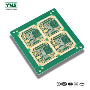
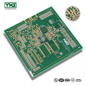
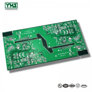
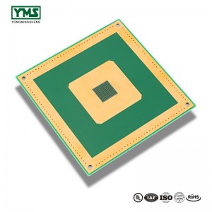
Yongmingsheng technology co., LTD. is a high-tech company integrating circuit board development, design, proofing, production (processing), testing, production and sales.
The main products are: aluminum base board, copper base board, PCB bare board, reasonable price;
Since the establishment of the company, from the original professional circuit board processing, to expand the production of flexible circuit board, rigid circuit board, etc. We have been making progress, we have been committed to become a high quality PCB manufacturer and service provider.
You May Like:
Post time: Sep-18-2019