
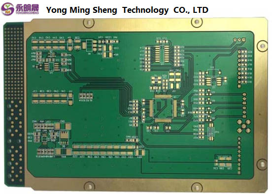
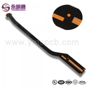
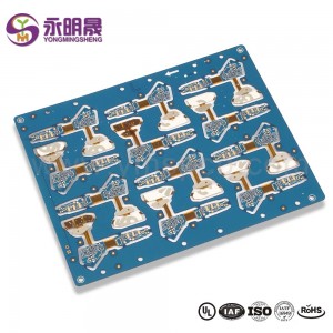
Edge Plating PCB 10 Layer Board edge plating PCB| YMS PCB

What is PCB Edge Plating?
PCB edge plating is the process of connecting the top and the bottom of the PCB by electroplating around the outer edges of the PCB. This process also can be named as sideplating, border plating, edge metalizing, or plated contour. For the devices with moderate or high requirements for EMC, signal integrity, and heat dissipation, edge plating has apparent advantages at negligible cost. Usually, ENIG or nickel-gold is recommended to be the surface finish method for the edge plating.
EDGE PLATING PCB PROCESS
Printed circuit board fabrication for edge soldering requires precision handling and faces many challenges around how plated edges are prepared and the lifetime adhesion of the plated material.
MCL has established industry practices and manufactures to these standards to ensure that our PCB edge castellation thoroughly prepares edge surfaces, applies the plated copper for immediate adhesion and processes the board to ensure long-term adhesion of every layer.
By using a controlled process in our circuit board fabrication for edge soldering, we can limit any potential hazard for through-holes and half-holes on the edge. The most significant concern is the creation of burrs, which will lead to the failure of mission-critical parts and can damage your equipment.
APPLICATIONS
Edge plating circuit boards are common in many industries, and edge plating is a common practice. You’ll find PCB edge castellation (or edge plating PCBs) applied in many cases, including:
Improving current-carrying capabilities
Edge connections and protection
Edge soldering to improve fabrication
Better support for connections such as boards that slide into metal casings
Please note that edge plating on printed circuit boards is a simple addition in many cases, but it requires specialized equipment and training. It’s an option for many different boards, but we always recommend taking this type of request to a manufacturer, like MCL, who has an established reputation of circuit board castellation.
We’ll be able to perform the right engineering checks to keep everything safe. For example, circuit board castellation should never cause the internal power planes to come to the edge of the board, because it can short the edge plating. When you travel, always mind the gap. When we perform circuit board fabrication for edge soldering, we always make sure there’s a gap before the edge plating. Edge plating helps to create a robust connection of the PCBs and can reduce the chance of device failures. Therefore, edge plating is widely used in applications where connections need to be better supported and becomes a common practice in PCB manufacturing. YMS provides professional equipment and specialized engineers to do the side plating process. Please send E-mail to us or contact our online services for more details about the edge plating process and design parameters.
Limitations
Because fabricators need to hold the circuit boards within the production panel in PCb prototype, they can’t plate the complete-length edge. Therefore, there are some gaps required to place rout tabs. It needs routing the circuit board profile at the place when fabricating the circuit boards with edge plating, and the edge plating is required before starting the process of through-hole plating, which remove v-cut scoring on a PCB that needs to undergo edge plating.
The edge plating PCB in YMS
With over 10 years as an industry leader, YMS has lots of manufacturing experience for PCB edge plating, and we are able to control high quality for edge plating without burrs. Because the satisfaction of customers is our goal, we will try our best to fabricate your board with the highest quality to meet your demands and committed to adhering to the strictest standards in PCB fabrication and assembly.
YMS, the electronic engineer’s best partner, is offering you low cost PCB fabrication with high quality.

You May Like:
1、How to make high frequency PCB
Video
Learn more about YMS products

What is edge plating in PCB?
You might have heard this concept called “edge plating” or “castellation,” which is the copper plating that runs from the top to the bottom surfaces of a PCB, and runs along at least one of the perimeter edges. PCB edge castellation ensures a strong connection through the board and limits the chance of equipment failures, especially in controlling protections for small form factor boards and sub-motherboards.
What is copper plating in PCB?
Copper plating is an electro-chemical process, in which a layer of copper is deposited on the metallic surface of a solid through the use of electric current.
Copper plating is an important process because:
It provides valuable corrosion protection.
It improves wear resistance of the surface.
It has excellent adhesion to most base metals, improving ductility of coated products.
It has excellent heat conductivity and electrical conductivity, making the plated products suitable for precision engineering applications, such as printed circuit boards (PCB).
Products categories
-
Thick Copper PCB 10 Layer (4OZ) High Tg Full B...
-
High Tg material PCB 6 Layer High Tg Board| YMS...
-

Wholesale Multi Layer PCB-PCB Manufacturer Chin...
-
Multilayer PCB manufacturing from 4 to 60 Layer...
-

LED display screen pcb HDI laser via in PAD cop...
-

Wholesale hard gold PCB multilayer Fr4 high TG ...


