
Wholesale Castellated Multilayer PCB from China | YMSPCB

When you create castellated holes on your многослойные платы ' edges, you can use them to replicate some parts of your PCB circuit. For example, if you have a circuit including a filter, feedback loops, or an inverter. You can mass-produce these little sub-circuits, test and solder them onto your main PCB, which contains the circuit’s remaining parts where needed.
The following are the uses of castellated holes.
You can use a castellated PCB as a breakout board for a specific portion of your larger многослойные печатные платы .
With castellated holes, you can easily change the component’s Pin layout with respect to user requirements.
You can produce integrated modules on one PCB board making use of a castellationthat can be further utilized into a different assembly while production is on.
It is easy to mount PCBs having castellated holes to a second PCB during the final production
Castellated holes are utilized in combining two boards in order to validate and ensure the quality of the solder joint.
They are utilized for small modules i.e. Wi-Fi modules or breakout boards
With castellated holes, the creation of wireless castellated circuit boards to the PCB links becomes easy
Castellated Holes Specifications
Depending on the need and final use of the board there are some design attributes that need to be met. For example:
· Size: It is recommended to use the largest possible size.
· Surface finish: Depends on the final use of the board, but ENIG is recommended.
· OL pad design: It is recommended to use the largest possible OL pad on top and bottom.
· Number of holes: This depends on the design; however, it is known that the less number of holes, the more difficult the PCB Assembly process will be.
Castellated Holes Application.
The holes on castellation PCBs are utilized in different industries. These include:
*Power
*Industrial control
*Computer application
*Consumer electronics (high end)
*Telecommunication
*Automobilesand more.
Узнать больше о продуктах YMS
Прочитать больше новостей

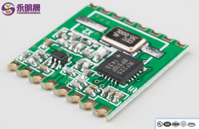
What Are Castellated Holes?
Castellations are plated through holes or vias located in the edges of a printed circuit board. Castellations are cut through to form a series of half holes. These half holes serve as pads intended to create a link between the module board and the board that it will be soldered onto.
What Are Castellated Holes Used For?
Castellated holes can be used for a couple of different reasons. Most commonly, they are used by designers to create PCB modules, such as Wi-Fi or Bluetooth modules, which will then be used as an independent part to be placed onto another board during the PCB assembly process. However, castellations are also used when combining two boards to ensure the solder inspection joint is properly structured and to create wireless PCB to PCB links.
Is 3 layer PCB possible?
Yes,It’s possible.
Which vias is used for multilayer PCB?
There are different types of PCB vias according to their functionality, however, the three most commonly used via are blind via, buried via as well as through hole. Plated through hole is the most common type of via, in fact, it is a hole dug completely through the multiple layers of a PCB.
How many layers are there in multilayer PCB?
4 – 22 layers standard, 30 layers advanced, 40 layers prototype.
What is Multilayer PCBs
Multilayer Printed Circuit Board, It is a type of PCB which comes with a combination of single sided PCB and double sided PCB. It features layers more than double sided PCB.
Печатная плата с особыми требованиями промышленности
Боковое покрытие печатной платы
Sideplating - это металлизация края платы в поле PCB. Кромка, Кайма, Металлический контур, Боковой металл - эти слова также могут использоваться для описания той же функции.
Половинные зубчатые отверстия
Castellations are plated through holes or vias located in the edges of a printed circuit board. are indentations created in the form of semi-plated holes on the edges of the PCB boards.These half holes serve as pads intended to create a link between the module board and the board that it will be soldered onto.
What is hard gold in PCB?
The Hard Gold surface finish, also known as Hard Electrolytic Gold, is composed of a layer of gold with added hardeners for increased durability, plated over a barrier coat of nickel using an electrolytic process.
What is hard gold plating?
Hard gold plating is a gold electrodeposit that has been alloyed with another element to alter the grain structure of the gold to achieve a harder deposit with a more refined grain structure. The most common alloying elements used in hard gold plating are cobalt, nickel or iron.Oct 4, 2017
What is the difference between Enig and hard gold?
ENIG plating is much softer than hard gold plating. Grain sizes are about 60 times larger with ENIG plating, and hardness runs between 20 and 100 HK25. ENIG plating holds up well at only 35 grams of contact force or less, and ENIG plating typically lasts for fewer cycles than hard plating.
категории товаров
-

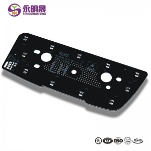
Светодиодный экран PCB HDI лазер через в PAD cop ...
-
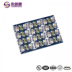
тяжелая медная печатная плата 4 слоя (4/4/4 / 4OZ) Черный Продано ...
-
Wholesale hard gold PCB multilayer Fr4 high TG ...
-
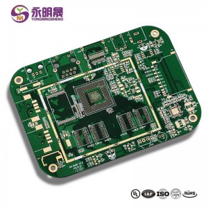
FR4 Multilayer PCB-Chian Wholesale Supplier | Y...
-

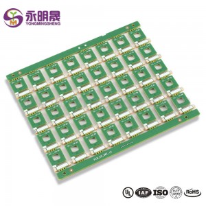
Китайская печатная плата 6Layer Gold Finger Blue Soldermask Bo ...
-
HDI Multilayer PCB-China PCB Manufacturer | YMSPCB


