
Wholesale hard gold PCB multilayer Fr4 high TG Factories in China| YMS PCB

Your reliabel hard gold PCB supplier
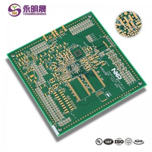
YMSPCB is a professional hard gold PCB supplier in China. We offer a wide range of PCBs widely used in intelligent industuial equipment, entertainment, intelligent AI, education robots, and more.
The YMSPCB hard gold PCB, also know as hard electrolytic gold, has a solid and durable surface. It provides extended shelf life and excellent performance. If you are looking for a highly durable board for high wear application, the YMSPCB is your best choice.
YMSPCB manufactures a hard gold PCB composed of a gold layer with added hardeners to increases durability. Another, using an electrolytic prcess, the board is plated with hard gold. During fabrication, the hard gold pcb als needs to be put with solder effectively.
Depending on your PCB design, we will consider other fabrication processes to ensure functionality and reliability. YMSPCB comes with many competitive advantages over different PCBs.
All YMSPCB hard gold PCB have are ISO cpmpliant, Rohs-certified, and UL-listed. We offer a comprehersive selection of products available in meticulous PCB quality management standards.
To maximize efficiency, you can send us your hard gold PCB drawing early to collaborate with our design and development team.
YMSPCB is capable of providing a one-stop solution for your product development. Being an expert manufacturer, we offer a high on-time rate and urgent delivery on your orders. We will help you maximize your opportunity to rocket your besiness in the market.
Full Body and Selective PCB Hard Gold Plating
The Hard Gold surface finish, also known as Hard Electrolytic Gold, is composed of a layer of gold with added hardeners for increased durability, plated over a barrier coat of nickel using an electrolytic process. Hard gold is extremely durable, so during PCB Fabrication this finish is usually applied to high-wear areas, such as edge connector Gold Fingers and keypads, since the hardness of the finish can withstand repeated use; however, due to the high cost of hard gold, and its relatively poor solder-ability, it is very rarely applied to solder-able areas.
Full Body Hard Gold is generally a rarely-chosen surface finish, where the full body of the PCB board is plated with hard gold. In order to apply a Full Body Hard Gold surface finish, an electrolytic process using an electric current or an immersion process is needed, depending on the PCB design. For Complete PCB Assembly projects, where we fabricate and assemble the boards, we will also need to consider the poor solderability of this finish; a very active flux will be required to solder effectively to the hard-gold-plated pad.
Pros
Hard, Durable Surface
No Lead
Very Long Shelf Life
Ons
Expensive
Extra Processing / Labor Intensive
Use of Resist / Tape
Plating / Bus Bars Required
Demarcation
Difficulty with Other Surface Finishes
Etching Undercut Leads to Slivering / Flaking
Not Solder-Able Above 17 μin
Finish Does Not Fully Encapsulate Trace Sidewalls, Except in Finger Areas
Important properties of hard gold finish
While selecting a hard gold finish, consider the following critical aspects:
Bonding considerations
The soldering of hard gold deposits is challenging due to the presence of non-noble elements like nickel, cobalt, etc. These metals oxidize at soldering temperatures and reduce the strength of the solder joint. Hence, this finish is not suitable for any kind of joining process.
For applications such as ultrasonic wire bonding, thermosonic bonding, etc. ENIG is preferred. The thickness and purity of gold are ideal for these processes.
Apperance
The appearance of hard gold plating is bright because of its refined grain structure. In light of this impression, it is an excellent choice for applications requiring cosmetically pleasing gold contacts, such as visible interconnect applications.
Corrosion resistance
Gold finish minimizes the corrosion resistance of the coating due to the added non-noble elements. It is easily oxidized at elevated temperatures.
Wear resistance
This finish consists of metallic elements like nickel, iron, or cobalt. Due to these elements, deposits develop finer grain structures that are more lustrous and resist sliding wear.
These are some factors that will help you determine the appropriate surface finish.
Узнайте больше о продуктах YMS

Прочитать больше новостей

What is hard gold PCB?
The Hard Gold surface finish, also known as Hard Electrolytic Gold, is composed of a layer of gold with added hardeners for increased durability, plated over a barrier coat of nickel using an electrolytic process.
what is hard gold plating?
Hard gold plating is a gold electrodeposit that has been alloyed with another element to alter the grain structure of the gold to achieve a harder deposit with a more refined grain structure. The most common alloying elements used in hard gold plating are cobalt, nickel or iron
How do you make hard gold PCB boards?
We first plate 3 – 6 microns of nickel onto the edge connector fingers and then on top of that 1 – 2 microns of hard gold. The plated gold is not 100% pure; it contains some cobalt to increase the wear-resistance of the surface.
What is gold plating in PCB?
Gold plating: Gold plating is a method of depositing a thin layer of gold onto the surface of another metal through plating way. The gold particles attached to the pcb, as strong adhesion also known as hard gold. The gold finger of memory bank is hard gold and abrasion resistant.
The difference between hard gold and soft gold
Goldplating can be divided into hard gold and soft gold. Because electroplated hard gold is alloy, its hardness is relatively hard, and it is suitable for use in places requiring force and friction. It is generally used as PCB side contact point (commonly known as gold finger). While soft gold is generally used for COB (Chip On Board) On the aluminum wire, or the contact surface of mobile phone keys, has recently been widely used in the BGA Board On both sides.
Glass Transition Temperature (Tg)—This is an important parameter for the base material, as it determines the temperature at which the resin matrix changes over from a firm, non-elastic condition to a soft, elastic one.
The difference between hard gold and soft gold is the composition of the layer of gold that is finally plated. When plating gold, you can choose to electroplate pure gold or alloy, because the hardness of pure gold is soft, so it is also called “soft gold”.
Full Body Hard Gold is generally a rarely-chosen surface finish, where the full body of the PCB board is plated with hard gold. In order to apply a Full Body Hard Gold surface finish, an electrolytic process using an electric current or an immersion process is needed, depending on the PCB design.
For Complete PCB Assembly projects, where we fabricate and assemble the boards, we will also need to consider the poor solderability of this finish; a very active flux will be required to solder effectively to the hard-gold-plated pad.
If you have any further questions about our PCB Surface Finish capabilities, or to get started on your project with YMS today, you can Contact Us over email at kell@ymspcb.com.
What is high Tg PCB (printed circuit board)
Normally high Tg refers to high heat resistance in PCB raw material, the standard Tg for copper clad laminate is between 130 – 140℃, High Tg is generally greater than 170℃, and middle Tg is generally greater than 150℃. Basically the printed circuit board with Tg≥170℃, we call high Tg PCB.
Hard Gold
▪ Usual thickness: 0.7 µm (0.00003”) to 1.3 µm (0.00005”) gold (99.7%) over 5.0
▪ µm (0.0002”) nickel or 0.2 µm (0.000008”) to 0.3 µm (0.00001”) gold (99.7%) over
▪ 5.0 µm (0.0002”) nickel for a solderable surface
▪ Very good for corrosion resistance
▪ Rated at 130-220 Knoop hardness
▪ Very good wear resistance
▪ Excellent for surface rotary switches, on-off contacts, and edge connectors
▪ Very good shelf life
категории товаров
-
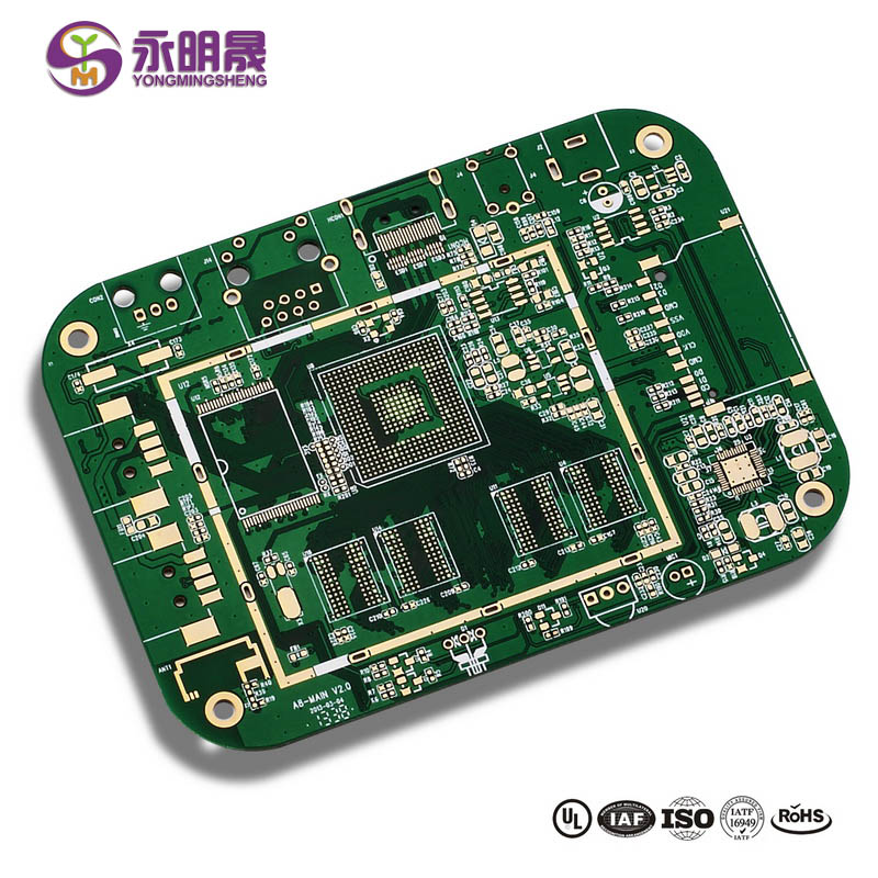
FR4 Multilayer PCB-Chian Wholesale Supplier | Y...
-

Светодиодный экран PCB HDI лазер через в PAD cop ...
-

Wholesale Multi Layer PCB-PCB Manufacturer Chin...
-
Печатная плата с высокой ТГ 6-слойная Печатная плата с высокой ТГ | YMS ...
-
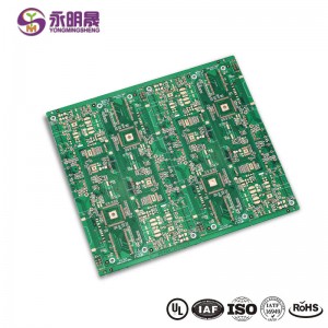
HDI Multilayer PCB-China PCB Manufacturer | YMSPCB
-
Multilayer PCB manufacturing from 4 to 60 Layer...


