
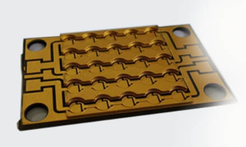
Extreme Copper PCB 2 Layer 10 0z Heavy Copper Board| YMS PCB

The construction of a heavy copper circuit endows a board with benefits such as:
- Increased endurance to thermal strains.
- Increased current carrying capacity.
- Increased mechanical strength at connector sites and in PTH holes.
- Use of exotic materials to their full potential without circuit failure.
- Reduced product size by incorporating multiple copper weights on the same layer of circuitry .
- Heavy copper plated vias carry higher current through the board and help to transfer heat to an external heatsink.
YMS重銅PCB製造機能:
| YMS重銅PCB製造機能の概要 | ||
| 特徴 | 機能 | |
| レイヤー数 | 1-30L | |
| 基材 | FR-4標準Tg、FR4-中Tg、FR4-高Tg | |
| 厚さ | 0.6 mm-8.0mm | |
| 外層の最大銅重量(完成) | 15OZ | |
| 内層の最大銅重量(完成) | 30OZ | |
| 最小線幅とスペース | 4オンスCu8mil / 8mil; 5オンスCu10mil / 10mil; 6オンスCu12mil / 12mil; 12オンスCu18mil / 28mil; 15オンスCu30mil / 38milなど | |
| BGAピッチ | 0.8mm(32mil) | |
| 最小機械ドリルサイズ | 0.25mm(10mil) | |
| スルーホールのアスペクト比 | 16:1 | |
| 表面仕上げ | HASL、鉛フリーHASL、ENIG、イマージョンスズ、OSP、イマージョンシルバー、ゴールドフィンガー、電気めっきハードゴールド、選択的OSP、ENEPIGなど。 | |
| 塗りつぶしオプション経由 | ビアは、導電性または非導電性エポキシのいずれかでメッキおよび充填されてから、キャップおよびメッキが施されます(VIPPO) | |
| 銅充填、銀充填 | ||
| 登録 | ±4mil | |
| 戦士の表情 | 緑、赤、黄、青、白、黒、紫、マットブラック、マットグリーンなど。 | |
あなたは好きかもしれません:
1、What are the precautions for heavy copper PCB wiring
2、What are the specifications of heavy copper PCB
3、What are the heavy copper PCB materials
YMS製品の詳細


ここにメッセージを書いて、私たちにそれを送ります


