
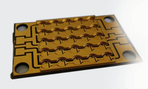
Extreme Copper PCB 2 Layer 10 0z Heavy Copper Board| YMS PCB

The construction of a heavy copper circuit endows a board with benefits such as:
- Increased endurance to thermal strains.
- Increased current carrying capacity.
- Increased mechanical strength at connector sites and in PTH holes.
- Use of exotic materials to their full potential without circuit failure.
- Reduced product size by incorporating multiple copper weights on the same layer of circuitry .
- Heavy copper plated vias carry higher current through the board and help to transfer heat to an external heatsink.
YMS Heavy Copper PCB Herstellungskapazitäten:
| Überblick über die Fertigungskapazitäten von YMS Heavy Copper PCB | ||
| Merkmal | Fähigkeiten | |
| Ebenenanzahl | 1-30L | |
| Basismaterial | FR-4 Standard-Tg, FR4-Mittel-Tg,FR4-Hoch-Tg | |
| Dicke | 0,6 mm - 8,0 mm | |
| Maximales Kupfergewicht der äußeren Schicht (fertig) | 15oz | |
| Maximales Kupfergewicht der inneren Schicht (fertig) | 30oz | |
| Minimale Linienbreite und Abstand | 4 Unzen Cu 8mil/8mil; 5oz Cu 10mil/10mil; 6oz Cu 12mil/12mil; 12oz Cu 18mil/28mil; 15oz Cu 30mil/38mil .etc. | |
| BGA PITCH | 0,8 mm (32 mil) | |
| Min. Mechanische Bohrgröße | 0,25 mm (10 mil) | |
| Seitenverhältnis für Durchgangsloch | 16: 1 | |
| Oberflächenfinish | HASL, bleifreies HASL, ENIG, Tauchdose, OSP, Immersionssilber, Goldfinger, Galvanisieren von Hartgold, selektives OSP , ENEPIG.etc. | |
| Über Fülloption | Die Durchkontaktierung wird plattiert und entweder mit leitendem oder nicht leitendem Epoxid gefüllt, dann abgedeckt und überzogen (VIPPO). | |
| Kupfer gefüllt, Silber gefüllt | ||
| Anmeldung | ± 4mil | |
| Lötmaske | Grün, Rot, Gelb, Blau, Weiß, Schwarz, Lila, Mattschwarz, Mattgrün usw. | |
Vielleicht gefällt dir:
1、What are the precautions for heavy copper PCB wiring
2、What are the specifications of heavy copper PCB
3、What are the heavy copper PCB materials
Erfahren Sie mehr über YMS-Produkte


Schreiben Sie hier Ihre Nachricht und senden Sie es uns


