
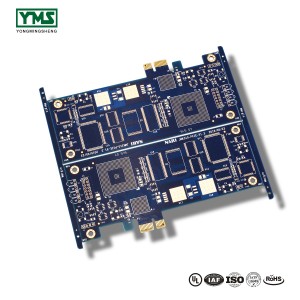
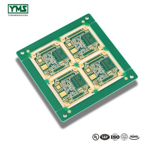
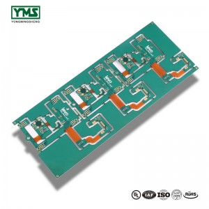
Factory best selling Multilayer Pcb Customized 6 Layers Control Hdi Pcb Circuit Board

To be able to ideal satisfy client’s requirements, all of our operations are strictly performed in line with our motto “High High-quality, Competitive Price tag, Fast Service” for Factory best selling Multilayer Pcb Customized 6 Layers Control Hdi Pcb Circuit Board, Our professional technological team will be wholeheartedly at your services. We sincerely welcome you to definitely take a look at our website and enterprise and send out us your inquiry.
To be able to ideal satisfy client’s requirements, all of our operations are strictly performed in line with our motto “High High-quality, Competitive Price tag, Fast Service” for Hdi Fr4 -tg Pcb, Hdi Multilayer Pcb, Hdi Pcb Circuit Board, Our professional engineering group will always be ready to serve you for consultation and feedback. We are able to also offer you with absolutely free samples to meet your requirements. Finest efforts will likely be produced to give you the ideal service and goods. For anyone who is thinking about our company and merchandise, please contact us by sending us emails or contact us quickly. As a way to know our merchandise and firm. lot more, you can come to our factory to find out it. We’ll always welcome guests from all over the world to our business to build company relations with us. Please feel free to get in touch with us for business and we believe we are going to share the top trading practical experience with all our merchants.
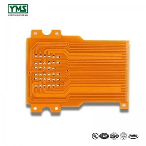
HDI Structures:
1+N+1 – PCBs contain 1 “build-up” of high-density interconnection layers.
i+N+i (i≥2) – PCBs contain 2 or more “build-up” of high density interconnection layers. Microvias on different layers can be staggered or stacked. Copper filled stacked microvia structures are commonly seen in challenging designs.
Any Layer HDI – All the layers of a PCB are high density interconnection layers which allows the conductors on any layer of the PCB to be interconnected freely with copper filled stacked microvia structures (“any layer via”). This provides a reliable interconnect solution for highly complex large pin-count device
Products categories
-
China OEM Customzized 5730 Led Aluminum Pcb,Led...
-
Popular Design for 4-layer Printed Circuit Boar...
-
Discountable price China High Tg Multilayer Rig...
-
Big Discount Double Sided Pcb,Prototype Pcb Car...
-
Wholesale Price China Medicine Machine Teflon P...
-
China Wholesale Shenzhen Custom Rigid-flex Prin...


