
New Fashion Design for 3 Step Hdi Pcb - 8Layer 2 Step HDI Board | YMS PCB – Yongmingsheng
New Fashion Design for 3 Step Hdi Pcb - 8Layer 2 Step HDI Board | YMS PCB – Yongmingsheng Detail:
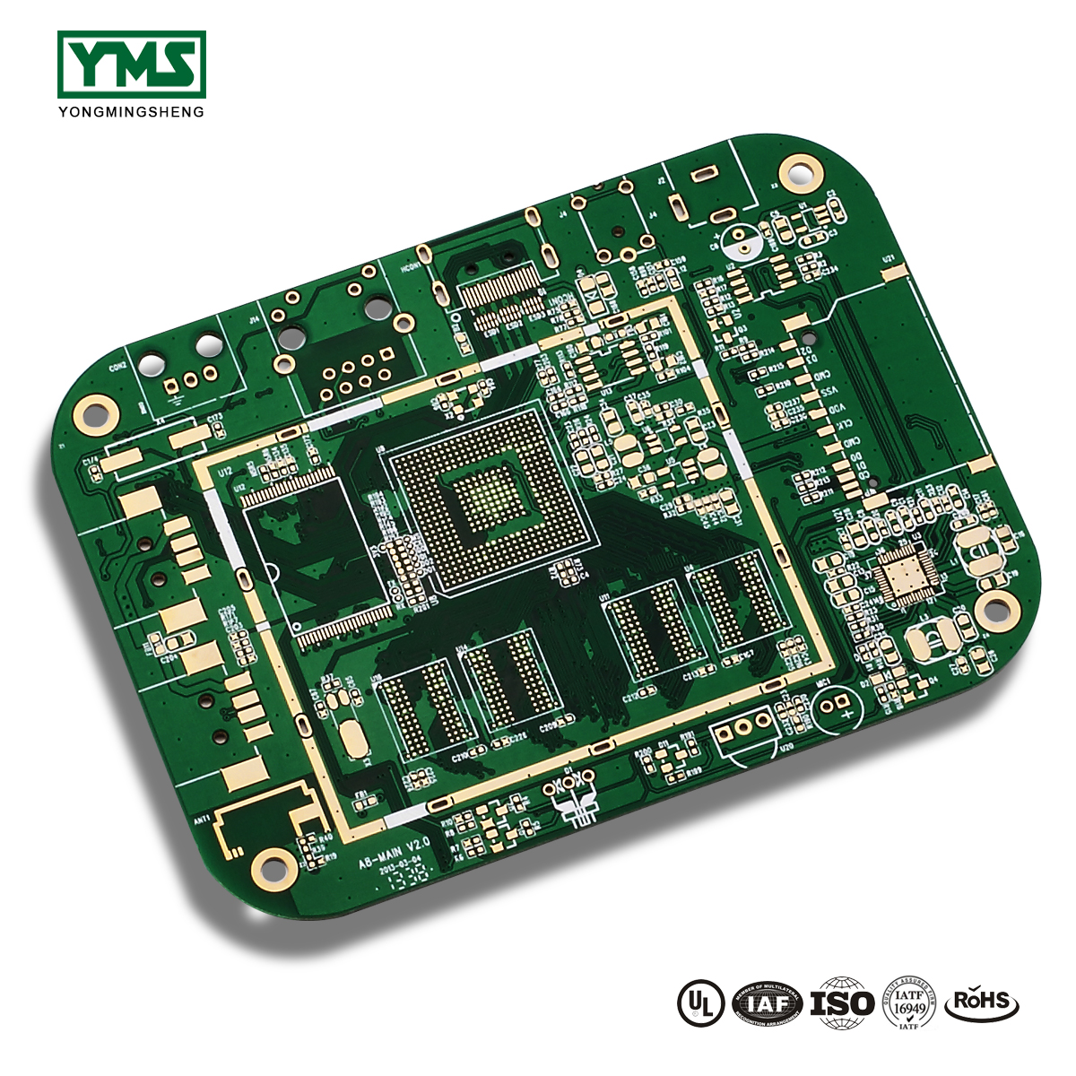
HDI Board production process:
At present, HDI board interconnection between layer and layer is mainly the following design: Staggered holes interconnection, Cross-layer interconnection, ladder interconnection and superposition holes interconnection. Among them, the superposition holes interconnection occupy the least space. There is a research suggests that reducing the number of through holes and increasing the number of blind holes can effectively improve the wiring density. And in the superposition interconnection, the methods of electroplating and resin plug are mainly used, especially the electroplating hole filling method which has more obvious advantages like high reliability and good conduction performance. Therefore, superposition interconnection is the most widely used design method for blind holes design. The process of stacking between layers is as follows: first blind hole is made, then second blind hole is made after lamination, then multi-blind hole is made according to this method, and the interconnection between layers is realized by electroplating hole filling method.
On the whole, the production process of HDI plate is complex, which needs to be completed after many times of production for a long time. It’s not only high requirements for the accuracy and shrinkage control of each layer, but also high standards in materials, equipment, environment and technical personnel.
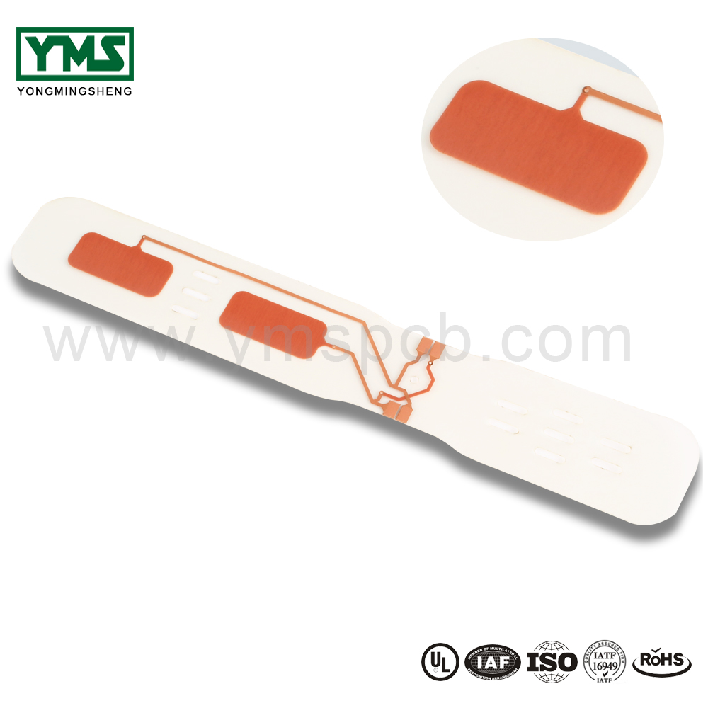
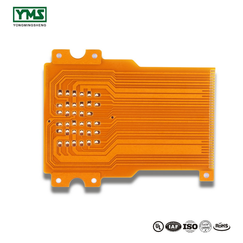
Product detail pictures:
Related Product Guide:
High Density Interconnect(HDI) PCBs Market Report Forecast by Industry Outlook, Capital Investment, Opportunities & Trends 2024 | Copper Base Board
N.S. court says FedEx Canada isn’t liable for lost package containing 50 rare coins | Copper Base Board
Well-run equipment, specialist income crew, and better after-sales services; We're also a unified major family, anyone stay with the organization value "unification, determination, tolerance" for New Fashion Design for 3 Step Hdi Pcb - 8Layer 2 Step HDI Board | YMS PCB – Yongmingsheng , The product will supply to all over the world, such as: Uzbekistan, France, Luxembourg, Corporate goal: Customers' satisfaction is our goal, and sincerely hope to establish long-terms stable cooperative relations with customers to jointly develop the market. Building brilliant tomorrow together!Our company regards "reasonable prices, efficient production time and good after-sales service" as our tenet. We hope to cooperate with more customers for mutual development and benefits. We welcome potential buyers to contact us.
As a veteran of this industry, we can say that the company can be a leader in the industry, select them is right.
Products categories
-
OEM/ODM Factory Cem-3 - Competitive Price for ...
-
Factory best selling Double Side Metal Core Pcb...
-
Rapid Delivery for Printed Circuit Board Design...
-
Well-designed Led Lighting Aluminum Pcb - Hot ...
-
factory customized Wonderful Rigid-Flex Pcb - ...
-
100% Original Factory Fingerprint Lock Rigid-Fl...


