Personlized Products China Gold finger HDI PCB, Control PCB Board Multilayer PCB Factory Offers Multilayer PCB Circuit Boards

We pursue the management tenet of "Quality is top-quality, Company is supreme, Status is first", and will sincerely create and share success with all shoppers for Personlized Products China 6 Layer HDI PCB, Control PCB Board Multilayer PCB Factory Offers Multilayer PCB Circuit Boards, We consider in top quality more than quantity. Before export in the hair there is strict quality control check during treatment as per international excellent standards.
We pursue the management tenet of "Quality is top-quality, Company is supreme, Status is first", and will sincerely create and share success with all shoppers for China 6 Layer PCB, Multi Layer PCB, Our company considers that selling is not only to gain profit but also popularize the culture of our company to the world. So we are working hard to give you the wholehearted service and willing to give you the most competitive price in the market
What is HDI PCB
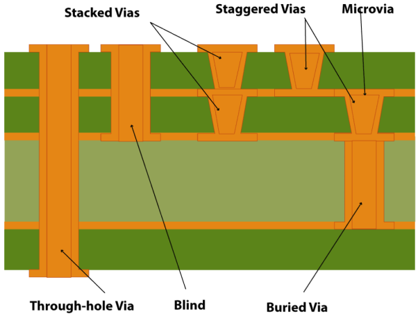
HDI PCB: High density interconnect PCB, are a way of making more room on your printed circuit board to make them more efficient and allow for faster transmission. It's relatively easy for most enterprising companies that are using printed circuit boards to see how this can benefit them.
Advantages of HDI PCB
The most common reason for using HDI technology is a significant increase in packaging density. The space obtained by finer track structures is available for components. Besides, overall space requirements are reduced will result in smaller board sizes and fewer layers.
Usually FPGA or BGA are available with 1mm or less spacing. HDI technology makes routing and connection easy, especially when routing between pins.
YMS HDI PCB manufacturing capabilities:
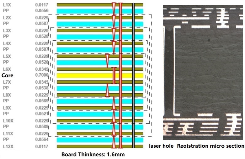
| YMS HDI PCB manufacturing capabilities overview | |
| Feature | capabilities |
| Layer Count | 4-60L |
| Available HDI PCB Technology | 1+N+1 |
| 2+N+2 | |
| 3+N+3 | |
| 4+N+4 | |
| 5+N+5 | |
| Any layer | |
| Thickness | 0.3mm-6mm |
| Minimum line Width and Space | 0.05mm/0.05mm(2mil/2mil) |
| BGA PITCH | 0.35mm |
| Min laser Drilled Size | 0.075mm(3nil) |
| Min mechanical Drilled Size | 0.15mm(6mil) |
| Aspect Ratio for laser hole | 0.9:1 |
| Aspect Ratio for through hole | 16:1 |
| Surface Finish | HASL, Lead free HASL,ENIG,Immersion Tin, OSP, Immersion Silver, Gold Finger, Electroplating Hard Gold, Selective OSP,ENEPIG.etc. |
| Via Fill Option | The via is plated and filled with either conductive or non-conductive epoxy then capped and plated over |
| Copper filled, silver filled | |
| Laser via copper plated shut | |
| Registration | ±4mil |
| Solder Mask | Green, Red, Yellow, Blue, White, Black, Purple, Matte Black, Matte green.etc. |
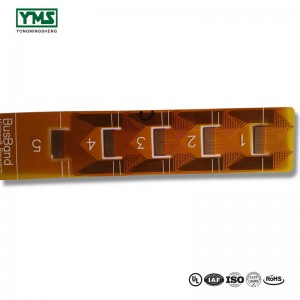
What is gold finger in PCB?
Gold finger is the connector at the edge of boards. It is similar to fingers, so we called gold finger, please see the following pictures. It is used to protect the printed circuit board prototypes from wear and tear. The surface treatment of the gold finger PCB.
What are gold fingers?
Gold Fingers are gold plated connectors on one edge of a printed circuit board. ... They must be hard in order to allow the circuit board to be inserted into a connector. They should also be very smooth and flat to allow for easy insertion. They are an excellent conductor which makes the connection much better.
What is gold on a circuit board?
Random Access Memory Chips (RAM) - A part of the circuit board, these little gold mines are installed to increase the operational memory of your computer. They often contain a small but a significant amount of gold-plated pins, and a thin layer of gold on their surfaces.


Board2-300x300.jpg)